Looking inside three-dimensional (3D) silicon photonic band gap crystals
Publication
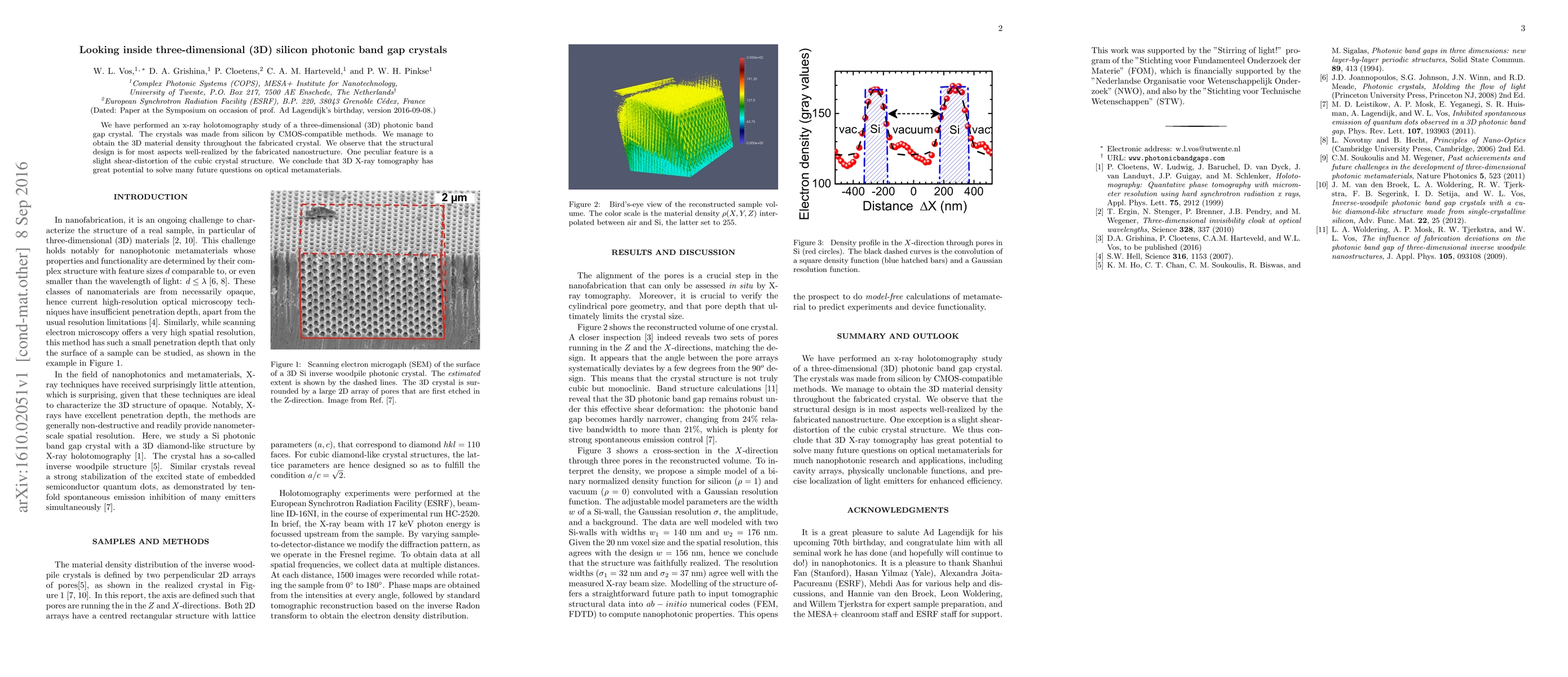
Metrics
AI Quick Summary
This study uses x-ray holotomography to examine a silicon-based 3D photonic band gap crystal fabricated via CMOS-compatible methods, revealing a slight shear-distortion in the cubic structure while confirming the overall structural design fidelity, highlighting the potential of 3D X-ray tomography for future optical metamaterials research.
Paper Preview
Abstract
We have performed an x-ray holotomography study of a three-dimensional (3D) photonic band gap crystal. The crystals was made from silicon by CMOS-compatible methods. We manage to obtain the 3D material density throughout the fabricated crystal. We observe that the structural design is for most aspects well-realized by the fabricated nanostructure. One peculiar feature is a slight shear-distortion of the cubic crystal structure. We conclude that 3D X-ray tomography has great potential to solve many future questions on optical metamaterials.
AI Key Findings
Get AI-generated insights about this paper's methodology, results, significance, and more — seven facets brought into focus.
Impact
Paper Details
PDF Preview
Key Terms
Citation Network
Current paper (gray), citations (green), references (blue)
Display is limited for performance on very large graphs.
Discussion 0