Publication
Metrics
AI Quick Summary
This paper investigates low-damage electron beam lithography techniques for nanostructuring Bi$_2$Te$_3$-class topological insulator thin films, revealing that 10 kV accelerating voltage minimizes damage while enabling the creation of 100 nm features with proper processing parameters. Higher voltages cause unacceptable damage, limiting the fabrication of nanodevices.
Paper Preview
Abstract
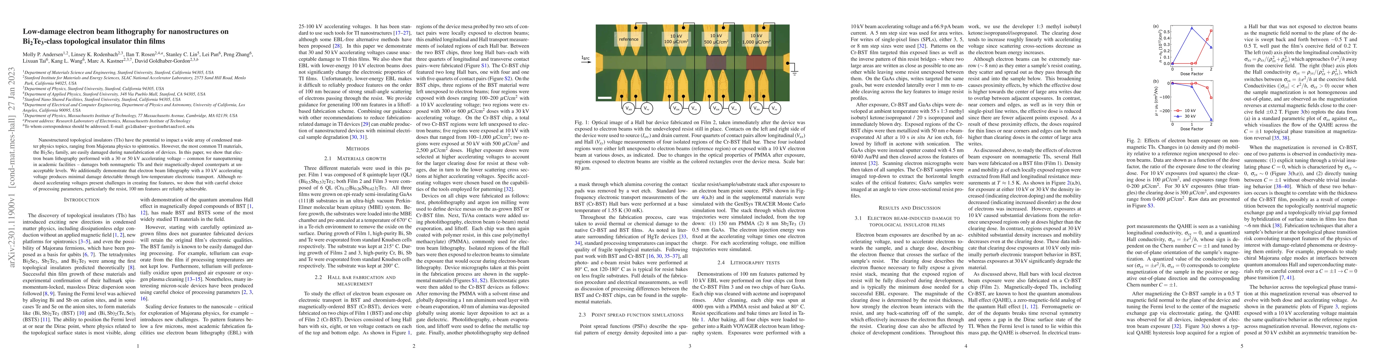
Nanostructured topological insulators (TIs) have the potential to impact a wide array of condensed matter physics topics, ranging from Majorana physics to spintronics. However, the most common TI materials, the Bi$_2$Se$_3$ family, are easily damaged during nanofabrication of devices. In this paper, we show that electron beam lithography performed with a 30 or 50 kV accelerating voltage -- common for nanopatterning in academic facilities -- damages both nonmagnetic TIs and their magnetically-doped counterparts at unacceptable levels. We additionally demonstrate that electron beam lithography with a 10 kV accelerating voltage produces minimal damage detectable through low-temperature electronic transport. Although reduced accelerating voltages present challenges in creating fine features, we show that with careful choice of processing parameters, particularly the resist, 100 nm features are reliably achievable.
AI Key Findings
Get AI-generated insights about this paper's methodology, results, significance, and more — seven facets brought into focus.
Impact
Paper Details
Authors
PDF Preview
Key Terms
Citation Network
Current paper (gray), citations (green), references (blue)
Display is limited for performance on very large graphs.
Discussion 0