ArxivLens

Publication

Published: Aug 11, 2025
Categories: physics.app-ph, cond-mat.mtrl-sci

Metrics

Source: ArXiv

AI Quick Summary

This research extends droplet etching epitaxy to In(Ga)As QDs in AlGaAs, enabling longer emission wavelengths while retaining advantages like low strain, controllable density, small FSS, and fast radiative decays. Key findings include QD densities of ~0.2 μm^-2, FSS of 3 μeV, and radiative lifetimes of ~300 ps, with emission range extended to ~920 nm at cryogenic temperatures, ideal for quantum photonics applications.

Quick Answers

What is "Low-density InGaAs/AlGaAs Quantum Dots in Droplet-Etched Nanoholes" about?

This research extends droplet etching epitaxy to In(Ga)As QDs in AlGaAs, enabling longer emission wavelengths while retaining advantages like low strain, controllable density, small FSS, and fast radiative decays. Key findings include QD densities of ~0.2 μm^-2, FSS of 3 μeV, and radiative lifetimes of ~300 ps, with emission range extended to ~920 nm at cryogenic temperatures, ideal for quantum photonics applications.

What methodology did the authors use?

The research utilizes droplet etching epitaxy to grow InGaAs/AlGaAs quantum dots, extending the emission wavelength range beyond GaAs/AlGaAs QDs while retaining beneficial properties such as low surface densities, small excitonic fine structure splitting, and fast radiative decays. More in Methodology →

What are the key results?

QD densities of ~0.2 μm^-2 achieved — FSS values as small as 3 μeV observed More in Key Results →

Why is this work significant?

These QDs are particularly suitable for integrated quantum photonics applications due to their low surface densities, small FSS, and fast radiative decays, offering advantages over conventional InGaAs/GaAs SK QDs. More in Significance →

What are the main limitations?

Higher spread in emission wavelength distribution for higher In content — FSS values, while small, are larger compared to recent GaAs QD works More in Limitations →

Paper Preview

Abstract

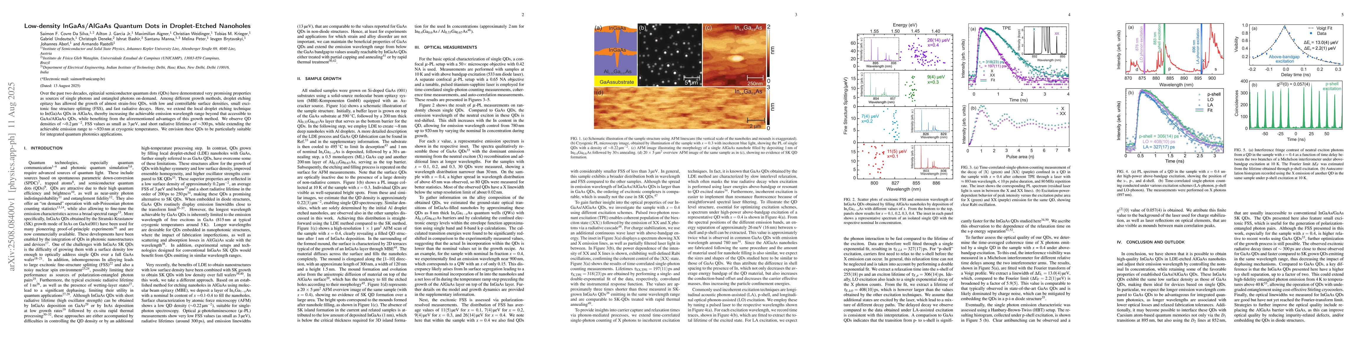
Over the past two decades, epitaxial semiconductor quantum dots (QDs) have demonstrated very promising properties as sources of single photons and entangled photons on-demand. Among different growth methods, droplet etching epitaxy has allowed the growth of almost strain-free QDs, with low and controllable surface densities, small excitonic fine structure splitting (FSS), and fast radiative decays. Here, we extend the local droplet etching technique to In(Ga)As QDs in AlGaAs, thereby increasing the achievable emission wavelength range beyond that accessible to GaAs/AlGaAs QDs, while benefiting from the aforementioned advantages of this growth method. We observe QD densities of $\sim 0.2\ \mu\mathrm{m}^{-2}$, FSS values as small as $3\ \mu\mathrm{eV}$, and short radiative lifetimes of $\sim 300\ \mathrm{ps}$, while extending the achievable emission range to $\sim 920\ \mathrm{nm}$ at cryogenic temperatures. We envision these QDs to be particularly suitable for integrated quantum photonics applications.
Key Findings, in focus

Seven facets of this paper, analysed and brought into focus by AI.

AI-generated · verify against source Generated Sep 03, 2025
In focus · one-line synthesis

These QDs are particularly suitable for integrated quantum photonics applications due to their low surface densities, small FSS, and fast radiative decays, offering advantages over conventional InGaAs/GaAs SK QDs.

01
MethodologyHow they did it

The research utilizes droplet etching epitaxy to grow InGaAs/AlGaAs quantum dots, extending the emission wavelength range beyond GaAs/AlGaAs QDs while retaining beneficial properties such as low surface densities, small excitonic fine structure splitting, and fast radiative decays.

02
ResultsWhat they found
  • QD densities of ~0.2 μm^-2 achieved
  • FSS values as small as 3 μeV observed
  • Short radiative lifetimes of ~300 ps measured
  • Emission range extended to ~920 nm at cryogenic temperatures
03
SignificanceWhy it matters

These QDs are particularly suitable for integrated quantum photonics applications due to their low surface densities, small FSS, and fast radiative decays, offering advantages over conventional InGaAs/GaAs SK QDs.

04
Technical ContributionsWhat's new technically

The study demonstrates high-quality InGaAs QDs in droplet-etched AlGaAs nanoholes with tunable emission wavelengths, retaining favorable properties of GaAs/AlGaAs QDs.

05
NoveltyWhat sets it apart

This work extends the emission range of almost strain-free QDs grown by droplet etching epitaxy to longer wavelengths, making them suitable for integrated quantum photonics applications.

06
LimitationsWhat to be cautious about
  • Higher spread in emission wavelength distribution for higher In content
  • FSS values, while small, are larger compared to recent GaAs QD works
07
Future WorkWhere it goes next
  • Further optimization of growth process to reduce FSS
  • Investigate interfacing with Caesium atom-based quantum memories

Paper Details

Paper ID: 2508.08400
Categories:
physics.app-ph cond-mat.mtrl-sci

How to Cite This Paper

Reference manager: RIS EndNote


Discussion 0

This website uses cookies to ensure you get the best experience. Learn more