Summary
$\mathrm{\beta}$-Gallium oxide ($\mathrm{\beta\mbox{-}Ga_{2}O_{3}}$) is an emerging widebandgap semiconductor for potential application in power and RF electronics applications. Initial theoretical calculation on a 2-dimensional electron gas (2DEG) in $\mathrm{\beta\mbox{-}(Al_{x}Ga_{1-x})_{2}O_{3}/Ga_{2}O_{3}}$ heterostructures show the promise for high speed transistors. However, the experimental results do not get close to the predicted mobility values. In this work, We perform more comprehensive calculations to study the low field 2DEG transport properties in the $\mathrm{\beta\mbox{-}(Al_{x}Ga_{1-x})_{2}O_{3}/Ga_{2}O_{3}}$ heterostructure. A self-consistent Poisson-Schrodinger simulation of heterostructure is used to obtain the subband energies and wavefunctions. The electronic structure, assuming confinement in a particular direction, and the phonon dispersion is calculated based on first principle methods under DFT and DFPT framework. Phonon confinement is not considered for the sake of simplicity. The different scattering mechanisms that are included in the calculation are phonon (polar and non-polar), remote impurity, alloy and interface-roughness. We include the full dynamic screening polar optical phonon screening. We report the temperature dependent low-field electron mobility.
AI Key Findings
Get AI-generated insights about this paper's methodology, results, and significance.
Paper Details
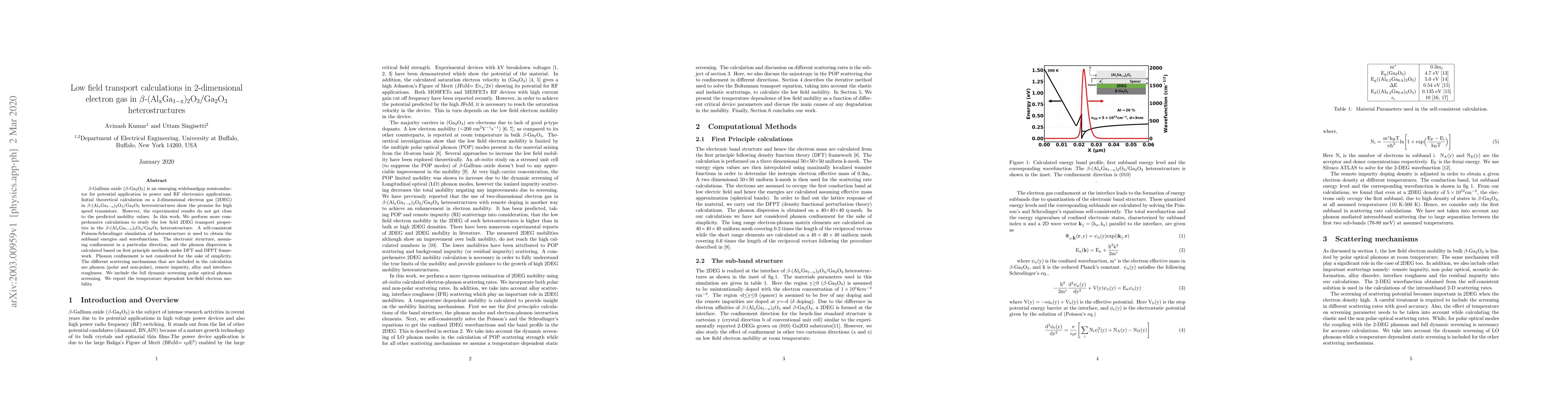
PDF Preview
Key Terms
Citation Network
Current paper (gray), citations (green), references (blue)
Display is limited for performance on very large graphs.
Similar Papers
Found 4 papersTailoring light holes in $β$-$Ga_{2}O_{3}$ via Anion-Anion Antibonding Coupling
Zhi Wang, Ke Xu, Rong Zhang et al.
Simultaneous study of acoustic and optic phonon scattering of electrons and holes in undoped $\mathrm{GaAs}$/$\mathrm{Al_{x} Ga_{1-x} As}$ heterostructures
C. Chen, D. A. Ritchie, P. Mehta et al.
No citations found for this paper.
Comments (0)