Publication
Metrics
AI Quick Summary
This paper reports the fabrication of low resistive edge contacts to CVD-grown graphene using CMOS compatible metals like Nickel and Aluminum, achieving significantly reduced contact resistance through optical lithography. The contact resistance is confirmed by Transfer Line Method and Kelvin Probe Force Microscopy.
Paper Preview
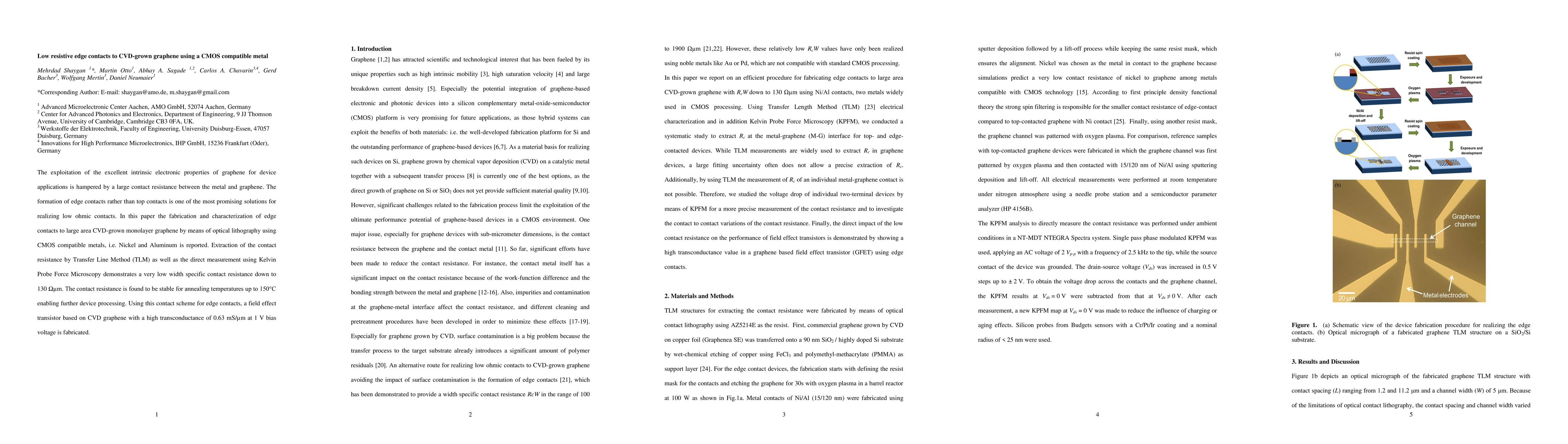
Abstract
The exploitation of the excellent intrinsic electronic properties of graphene for device applications is hampered by a large contact resistance between the metal and graphene. The formation of edge contacts rather than top contacts is one of the most promising solutions for realizing low ohmic contacts. In this paper the fabrication and characterization of edge contacts to large area CVD-grown monolayer graphene by means of optical lithography using CMOS compatible metals, i.e. Nickel and Aluminum is reported. Extraction of the contact resistance by Transfer Line Method (TLM) as well as the direct measurement using Kelvin Probe Force Microscopy demonstrates a very low width specific contact resistance.
AI Key Findings
Get AI-generated insights about this paper's methodology, results, significance, and more — seven facets brought into focus.
Impact
Paper Details
PDF Preview
Key Terms
Citation Network
Current paper (gray), citations (green), references (blue)
Display is limited for performance on very large graphs.
Discussion 0