Summary
The low temperature electrical behavior of adjacent silicide/Si Schottky contacts with or without dopant segregation is investigated. The electrical characteristics are very well modeled by thermionic-field emission for non-segregated contacts separated by micrometer-sized gaps. Still, an excess of current occurs at low temperature for short contact separations or dopant-segregated contacts when the voltage applied to the device is sufficiently high. From two-dimensional self-consistent non-equilibrium Green's function simulations, the dependence of the Schottky barrier profile on the applied voltage, unaccounted for in usual thermionic-field emission models, is found to be the source of this deviation.
AI Key Findings
Generated Sep 06, 2025
Methodology
A 2D self-consistent NEGF simulation approach was used to investigate the impact of V on the energy band profile and current characteristics of dopant-segregated Schottky structures.
Key Results
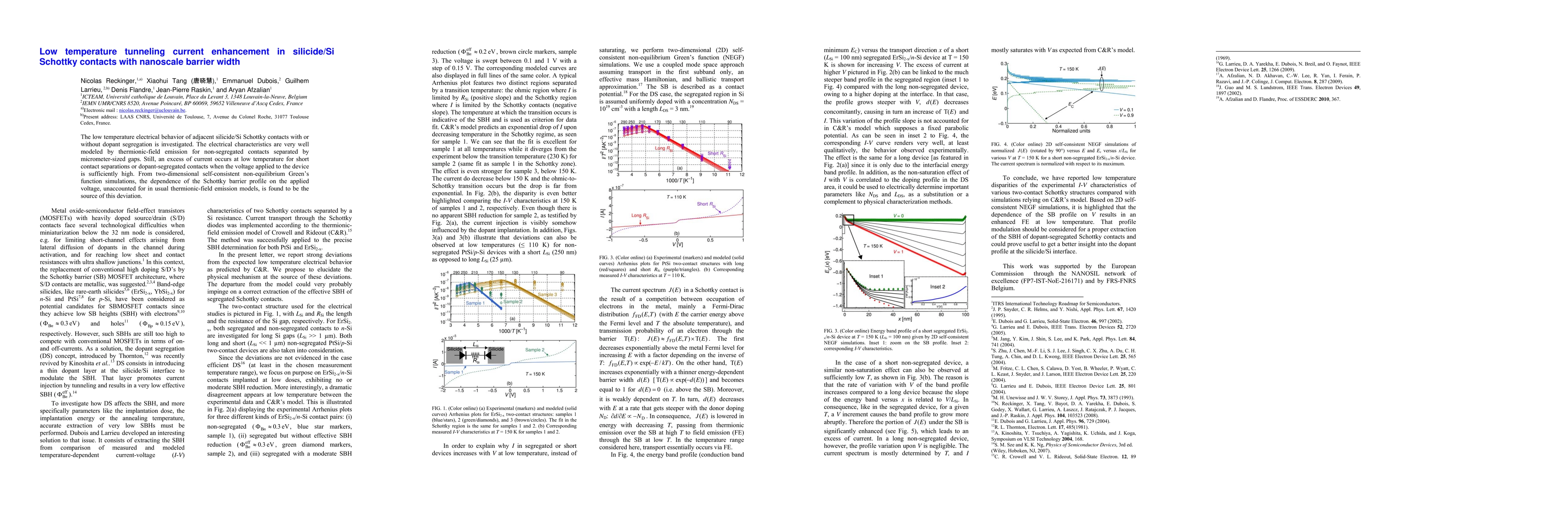
- The dependence of the SB profile on V results in an enhanced FE at low temperature.
- The non-saturation effect of I with V is correlated to the doping profile in the DS area.
- The current spectrum is mostly determined by T, and I mostly saturates with V as expected from C\u00e2\u0237\u2019s model.
Significance
This work highlights the importance of considering the dependence of the SB profile on V for proper extraction of the SBH of dopant-segregated Schottky contacts.
Technical Contribution
The 2D self-consistent NEGF simulation approach provides a new tool for investigating the impact of V on the energy band profile and current characteristics of dopant-segregated Schottky structures.
Novelty
This work presents a novel approach to understanding the impact of V on the energy band profile and current characteristics of dopant-segregated Schottky structures, which is different from existing research.
Limitations
- The simulations were limited to a specific device structure and doping profile.
- The experimental data used in this study may not be representative of all dopant-segregated Schottky structures.
Future Work
- Investigating the impact of different device structures and doping profiles on the energy band profile and current characteristics.
- Experimental verification of the theoretical findings using high-quality experimental data.
Paper Details
PDF Preview
Key Terms
Citation Network
Current paper (gray), citations (green), references (blue)
Display is limited for performance on very large graphs.
Similar Papers
Found 4 papers| Title | Authors | Year | Actions |
|---|
Comments (0)