The research employs luminescence thermometry using erbium emitters integrated into nanophotonic silicon waveguides, studying thermal activation of non-radiative decay channels above 200 K and thermal depopulation of spin- and crystal field levels at lower temperatures.
Publication
Metrics
AI Quick Summary
This paper presents an innovative luminescence thermometry technique using erbium emitters integrated into nanophotonic silicon waveguides for precise temperature measurement across a wide range from 295 K to 2 K. The method achieves high sensitivity and precision, with potential for further optimization to reduce measurement times and enhance spatial resolution.
Quick Answers
What methodology did the authors use?
The research employs luminescence thermometry using erbium emitters integrated into nanophotonic silicon waveguides, studying thermal activation of non-radiative decay channels above 200 K and thermal depopulation of spin- and crystal field levels at lower temperatures. More in Methodology →
What are the key results?
Achieved sensitivity of 0.22(4) %/K at room temperature, increasing to 420(50) %/K at approximately 2 K. — Measurement precision ranges from 0.04(1) K at the lowest studied temperature to 6(1) K at ambient conditions within a few-minute interval. More in Key Results →
Why is this work significant?
This work presents a novel approach to precise temperature measurement within nanophotonic devices, crucial for classical and quantum technologies, with spatial resolution down to a few nanometers. More in Significance →
What are the main limitations?
The method's sensitivity decreases below 10 K due to reduced signal levels and saturation of phonon broadening. — Thermalization of the spin state can be impeded by long spin-lattice relaxation times, especially at low temperatures and high magnetic fields. More in Limitations →
Abstract
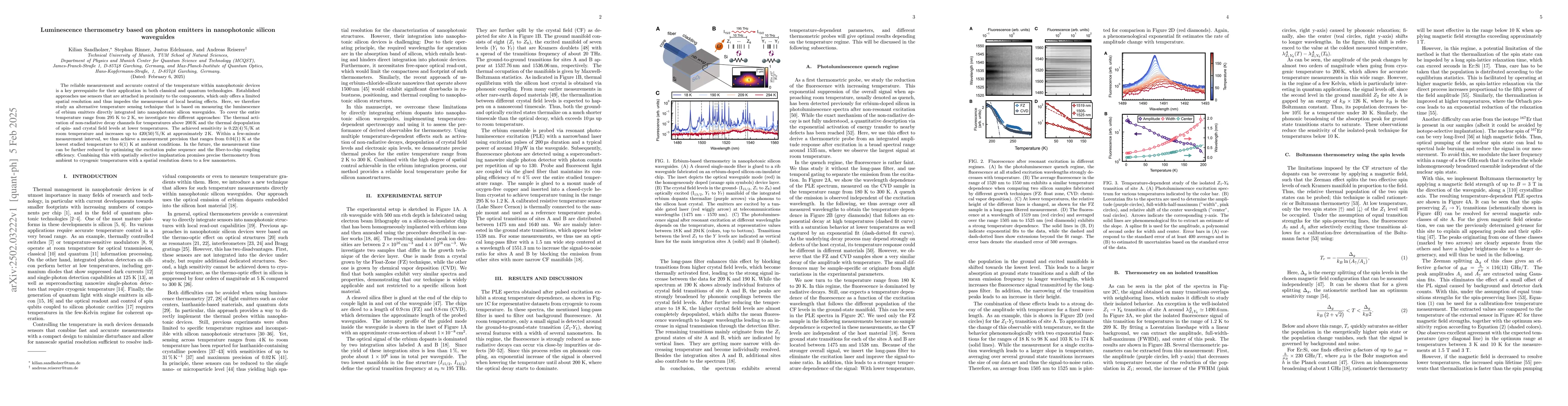
The reliable measurement and accurate control of the temperature within nanophotonic devices is a key prerequisite for their application in both classical and quantum technologies. Established approaches use sensors that are attached in proximity to the components, which only offers a limited spatial resolution and thus impedes the measurement of local heating effects. Here, we therefore study an alternative temperature sensing technique that is based on measuring the luminescence of erbium emitters directly integrated into nanophotonic silicon waveguides. To cover the entire temperature range from 295 K to 2 K, we investigate two different approaches: The thermal activation of non-radiative decay channels for temperatures above 200 K and the thermal depopulation of spin- and crystal field levels at lower temperatures. The achieved sensitivity is 0.22(4) %/K at room temperature and increases up to 420(50) %/K at approximately 2 K. Within a few-minute measurement interval, we thus achieve a measurement precision that ranges from 0.04(1) K at the lowest studied temperature to 6(1) K at ambient conditions. In the future, the measurement time can be further reduced by optimizing the excitation pulse sequence and the fiber-to-chip coupling efficiency. Combining this with spatially selective implantation promises precise thermometry from ambient to cryogenic temperatures with a spatial resolution down to a few nanometers.
Key Findings, in focus
Seven facets of this paper, analysed and brought into focus by AI.
This work presents a novel approach to precise temperature measurement within nanophotonic devices, crucial for classical and quantum technologies, with spatial resolution down to a few nanometers.
- Achieved sensitivity of 0.22(4) %/K at room temperature, increasing to 420(50) %/K at approximately 2 K.
- Measurement precision ranges from 0.04(1) K at the lowest studied temperature to 6(1) K at ambient conditions within a few-minute interval.
- Demonstrated temperature-dependent study of the isolated Z1-Y6 transition of site A, extracting thermometric parameters like amplitude, full-width-half-maximum, and center shift.
- Implemented Boltzmann thermometry using spin levels, providing calibration-free temperature measurement with high sensitivity below 10 K under magnetic fields exceeding approximately 1 T.
This work presents a novel approach to precise temperature measurement within nanophotonic devices, crucial for classical and quantum technologies, with spatial resolution down to a few nanometers.
The paper introduces a new luminescence thermometry technique based on integrated photon emitters in nanophotonic silicon waveguides, offering high precision and spatial resolution.
This research presents an innovative method for temperature sensing directly within nanophotonic devices, overcoming limitations of external sensors by integrating photon emitters and utilizing both thermal activation and spin-level depopulation for temperature sensing across a wide range.
- The method's sensitivity decreases below 10 K due to reduced signal levels and saturation of phonon broadening.
- Thermalization of the spin state can be impeded by long spin-lattice relaxation times, especially at low temperatures and high magnetic fields.
- Further reduce measurement time by optimizing excitation pulse sequences and fiber-to-chip coupling efficiency.
- Combine spatially selective implantation for precise thermometry from ambient to cryogenic temperatures.
Impact
Authors
PDF Preview
Citation Network
Current paper (gray), citations (green), references (blue)
Display is limited for performance on very large graphs.
Discussion 0