Making BaZrS3 chalcogenide perovskite thin films by molecular beam epitaxy
Publication
Metrics
AI Quick Summary
This paper demonstrates the fabrication of high-quality BaZrS3 chalcogenide perovskite thin films via molecular beam epitaxy, showing smooth atomic-scale films with near-perfect stoichiometry and sharp interfaces, and identifying two competing growth modes for epitaxial growth. The findings pave the way for tunable semiconductor properties and revive gas-source chalcogenide MBE techniques.
Paper Preview
Abstract
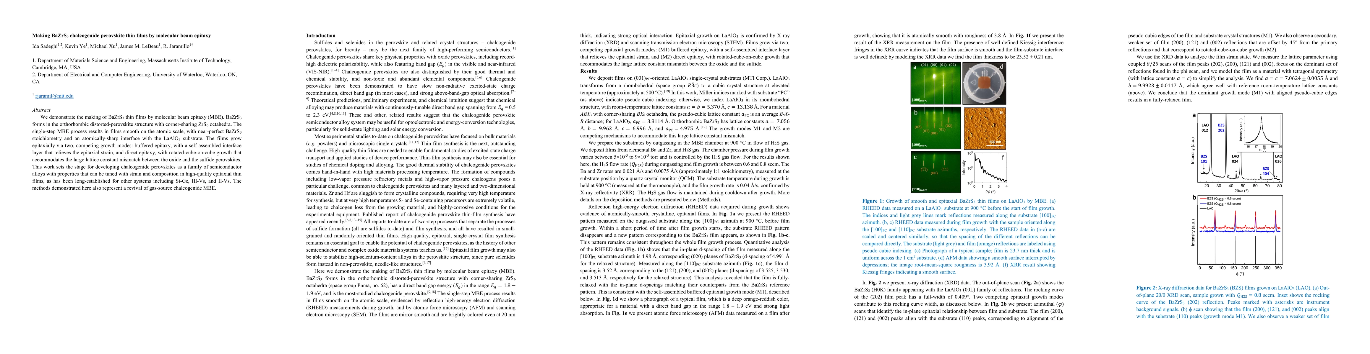
We demonstrate the making of BaZrS3 thin films by molecular beam epitaxy (MBE). BaZrS3 forms in the orthorhombic distorted-perovskite structure with corner-sharing ZrS6 octahedra. The single-step MBE process results in films smooth on the atomic scale, with near-perfect BaZrS3 stoichiometry and an atomically-sharp interface with the LaAlO3 substrate. The films grow epitaxially via two, competing growth modes: buffered epitaxy, with a self-assembled interface layer that relieves the epitaxial strain, and direct epitaxy, with rotated-cube-on-cube growth that accommodates the large lattice constant mismatch between the oxide and the sulfide perovskites. This work sets the stage for developing chalcogenide perovskites as a family of semiconductor alloys with properties that can be tuned with strain and composition in high-quality epitaxial thin films, as has been long-established for other systems including Si-Ge, III-Vs, and II-Vs. The methods demonstrated here also represent a revival of gas-source chalcogenide MBE.
AI Key Findings
Get AI-generated insights about this paper's methodology, results, significance, and more — seven facets brought into focus.
Impact
Paper Details
Authors
PDF Preview
Key Terms
Citation Network
Current paper (gray), citations (green), references (blue)
Display is limited for performance on very large graphs.
Discussion 0