Maximal single-frequency electromagnetic response
Publication
Metrics
Paper Preview
Abstract
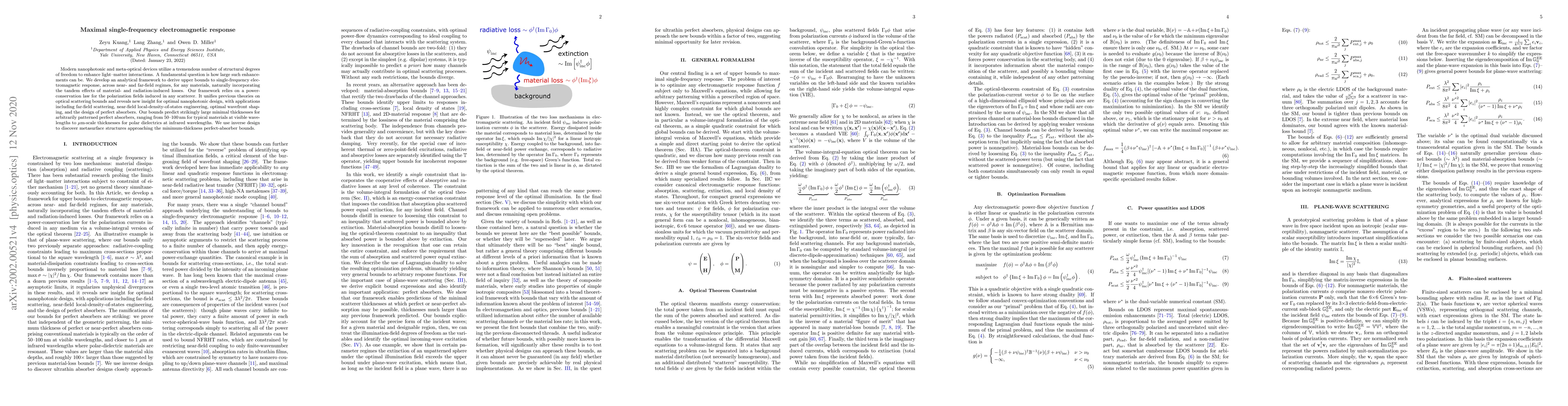
Modern nanophotonic and meta-optical devices utilize a tremendous number of structural degrees of freedom to enhance light--matter interactions. A fundamental question is how large such enhancements can be. We develop an analytical framework to derive upper bounds to single-frequency electromagnetic response, across near- and far-field regimes, for any materials, naturally incorporating the tandem effects of material- and radiation-induced losses. Our framework relies on a power-conservation law for the polarization fields induced in any scatterer. It unifies previous theories on optical scattering bounds and reveals new insight for optimal nanophotonic design, with applications including far-field scattering, near-field local-density-of-states engineering, optimal wavefront shaping, and the design of perfect absorbers. Our bounds predict strikingly large minimal thicknesses for arbitrarily patterned perfect absorbers, ranging from 50--100 nm for typical materials at visible wavelengths to micrometer-scale thicknesses for polar dielectrics at infrared wavelengths. We use inverse design to discover metasurface structures approaching the minimum-thickness perfect-absorber bounds.
AI Key Findings
Get AI-generated insights about this paper's methodology, results, significance, and more — seven facets brought into focus.
Impact
Paper Details
Authors
PDF Preview
Key Terms
Citation Network
Current paper (gray), citations (green), references (blue)
Display is limited for performance on very large graphs.
Discussion 0