Maximizing absorption in photon trapping ultra-fast silicon photodetectors
Publication
Metrics
AI Quick Summary
This paper investigates strategies to enhance photon trapping in silicon photodetectors, achieving a 1000% broadband absorption improvement and 50% capacitance reduction. It proposes empirical equations linking photodetector efficiency with trapping structure design and fabrication limitations, paving the way for cost-effective CMOS integration.
Paper Preview
Abstract
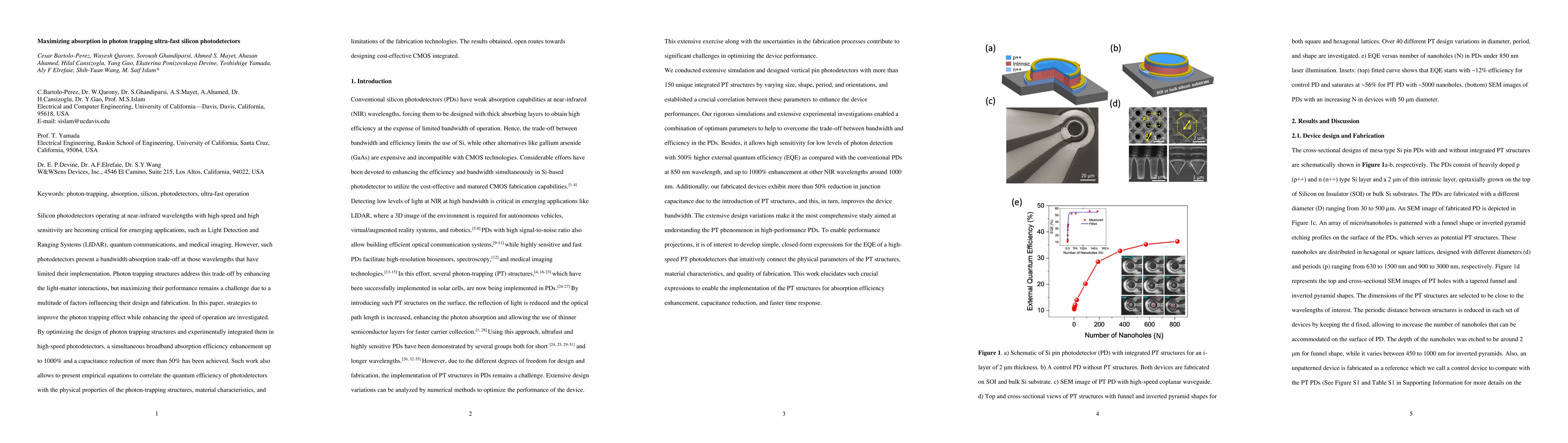
Silicon photodetectors operating at near-infrared wavelengths with high-speed and high sensitivity are becoming critical for emerging applications, such as Light Detection and Ranging Systems (LIDAR), quantum communications, and medical imaging. However, such photodetectors present a bandwidth-absorption trade-off at those wavelengths that have limited their implementation. Photon trapping structures address this trade-off by enhancing the light-matter interactions, but maximizing their performance remains a challenge due to a multitude of factors influencing their design and fabrication. In this paper, strategies to improve the photon trapping effect while enhancing the speed of operation are investigated. By optimizing the design of photon trapping structures and experimentally integrated them in high-speed photodetectors, a simultaneous broadband absorption efficiency enhancement up to 1000% and a capacitance reduction of more than 50% has been achieved. Such work also allows to present empirical equations to correlate the quantum efficiency of photodetectors with the physical properties of the photon-trapping structures, material characteristics, and limitations of the fabrication technologies. The results obtained, open routes towards designing cost-effective CMOS integrated.
AI Key Findings
Get AI-generated insights about this paper's methodology, results, significance, and more — seven facets brought into focus.
Impact
Paper Details
Authors
PDF Preview
Key Terms
Citation Network
Current paper (gray), citations (green), references (blue)
Display is limited for performance on very large graphs.
Discussion 0