01
MethodologyHow they did it
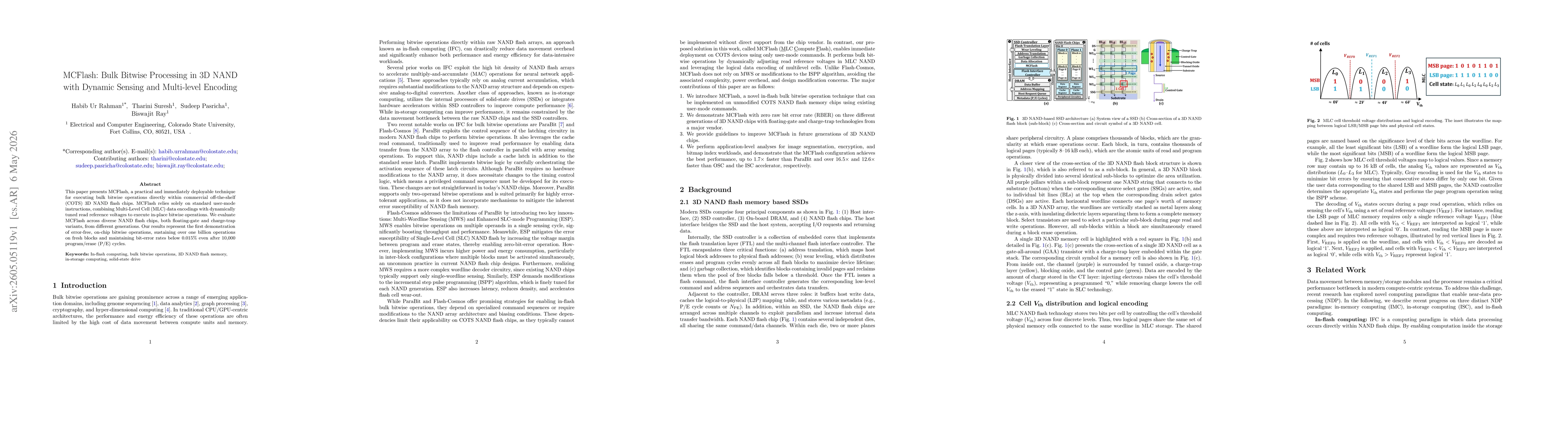
MCFlash leverages standard user-mode instructions to perform in-place bulk bitwise operations directly inside 3D NAND flash by combining Multi-Level Cell (MLC) data encodings with dynamically tuned read reference voltages, evaluated across diverse floating-gate and charge-trap NAND chips from multiple generations to demonstrate error-free, on-chip bitwise processing.
Discussion 0