This paper investigates the mobility measurements in dual-gated MoS2 transistors, highlighting the significant discrepancy in mobility values when using back-gated versus top-gated configurations. The study suggests that the overestimation of mobility in dual-gated devices may be due to measurement techniques rather than surface quality differences.
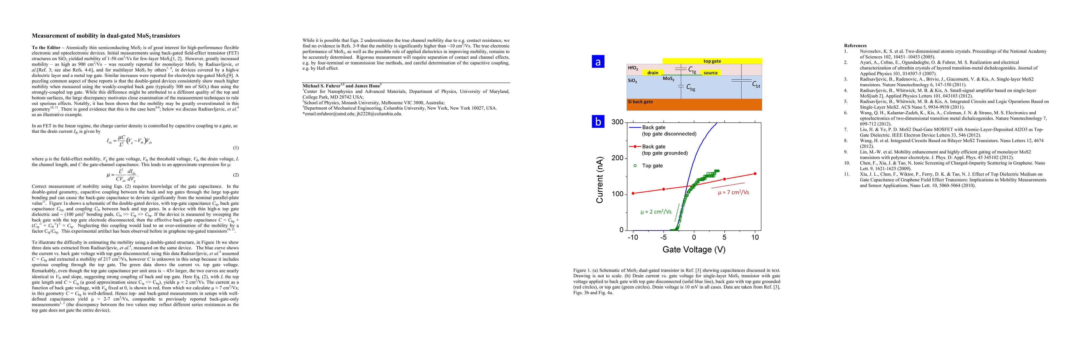
Atomically thin semiconducting MoS2 is of great interest for high-performance flexible electronic and optoelectronic devices. Initial measurements using back-gated field-effect transistor (FET) structures on SiO2 yielded mobility of 1-50 cm^2/Vs for few-layer MoS2[1, 2]. Initial measurements using back-gated field-effect transistor (FET) structures on SiO2 yielded mobility of 1-50 cm^2/Vs for few-layer MoS2[1, 2]. However, greatly increased mobility - as high as 900 cm^2/Vs - was recently reported for monolayer MoS2 by Radisavljevic, et al.[Ref. 3; see also Refs. 4-6], and for multilayer MoS2 by others[7, 8], in devices covered by a high-kappa dielectric layer and a metal top gate. Similar increases were reported for electrolyte top-gated MoS2[9]. A puzzling common aspect of these reports is that the double-gated devices consistently show much higher mobility when measured using the weakly-coupled back gate (typically 300 nm of SiO2) than using the strongly-coupled top gate. While this difference might be attributed to a different quality of the top and bottom surfaces, the large discrepancy motivates close examination of the measurement techniques to rule out spurious effects. Notably, it has been shown that the mobility may be greatly overestimated in this geometry[10, 11]. There is good evidence that this is the case here[4-9]; below we discuss Radisavljevic, et al.[4] as an illustrative example.
This graph shows how this paper is connected to other research. The current paper is shown in dark gray, papers that cite it are in green, and papers it references are in blue. You can:
• Hover over any node to see the paper title
• Click a node to view that paper's details
• Drag nodes to rearrange the graph
• Use the zoom controls (bottom right) to zoom in/out
Title | Authors | Year | Actions |
---|---|---|---|
Substrate-induced modulation of transient optical response of large-area monolayer MoS2
|
Ashish Soni, Nagendra S. Kamath, Yun-Yang Shen, Harshita Seksaria, Abir De Sarkar, Wen-Hao Chang, S. Pal
|
2025
|
View Paper |
Programmable WSe2 2D Lateral p‐n Junctions Controlled by Dual Floating Gates
|
Nuertai Jiazila, Peng Song, Chijun Wei, Xuanye Liu, Hui Gao, Jiequn Sun, Chengze Du, Hui Guo, Haitao Yang, Lihong Bao, Hong-Jun Gao
|
2025
|
View Paper |
Interfaces in two-dimensional transistors: Key to pushing performance and integration
|
Chang Liu, Shuaiqin Wu, Ying Zhang, Xudong Wang, Junhao Chu, Jianlu Wang
|
2025
|
View Paper |
Quantum mechanical insights into Edge-Dependent electronic properties of phosphorene nanoribbons
|
M. Bazrafshan, A. Vatankhahan, F. Khoeini, Omid Farzadian
|
2025
|
View Paper |
Two-Dimensional Organic-Inorganic van der Waals Hybrids.
|
Fucai Cui, Víctor García-López, Zhiyong Wang, Zhongzhong Luo, Daowei He, Xinliang Feng, Renhao Dong, Xinran Wang
|
2024
|
View Paper |
Theoretical Threshold Voltage of Two-Dimensional Semiconductor Field-Effect Transistors
|
Daoyu Zhang, Yinhao Zhao, Minnan Yang
|
2024
|
View Paper |
Bi-MoSe2 Contacts in the Ultraclean Limit: Closing the Theory-Experiment Loop.
|
Yang Liu, Song Liu, Zhiying Wang, Ashraf Hasan Mohammad Al-Bqerat, A. Zangiabadi, V. Perebeinos, James C Hone
|
2024
|
View Paper |
Axially‐Polarized Excitonic Series and Anisotropic van der Waals Stacked Heterojunction in a Quasi‐1D Layered Transition‐Metal Trichalcogenide
|
Adzilah Shahna Rosyadi, Ying-Xuan Lin, Yu-Hung Peng, Ching-Hwa Ho
|
2024
|
View Paper |
Gas-sensing performance of WS2/WO3 binary thin films for methane and hydrogen detection
|
R. Salamatizadeh, M. Adelifard, S. A. Ketabi
|
2024
|
View Paper |
Electrical transport crossover and large magnetoresistance in selenium deficient van der Waals
<mml:math xmlns:mml="http://www.w3.org/1998/Math/MathML"><mml:mrow><mml:msub><mml:mi>HfSe</mml:mi><mml:mrow><mml:mn>2</mml:mn><mml:mtext>−</mml:mtext><mml:mi>x</mml:mi></mml:mrow></mml:msub></mml:mrow></m
|
Wenhao Liu, Yangzi Zheng, A. Kondusamy, David L. Scherm, A. Malko, Bing Lv
|
2024
|
View Paper |
Enhancing Carrier Mobility in Monolayer MoS2 Transistors with Process-Induced Strain.
|
Yue Zhang, He Lin Zhao, Siyuan Huang, M. Hossain, A. M. van der Zande
|
2024
|
View Paper |
Strain tunable optical and transport properties of intrinsic ferromagnetic semiconductor CrOCl monolayer
|
Xiaolei Li, Hongmei Zhang, Zichen Tao, Yanyan Huang, Zhengchao Dong, Dayong Liu, C. Zhong, H. Fu
|
2024
|
View Paper |
First-principles study of carrier mobility and strain effect in MX (M=Sn, Pb; X=P, As) monolayers
|
Bo Zhang, W. Wan, Yong Liu, Yanfeng Ge
|
2024
|
View Paper |
Side‐Gate BN‐MoS2 Transistor for Reconfigurable Multifunctional Electronics
|
Daobing Zeng, Rongxiang Ding, Guanyu Liu, Huihui Lu, Miao Zhang, Z. Xue, Ziao Tian, Zengfeng Di
|
2023
|
View Paper |
Recent Progress on Phase Engineering of Nanomaterials.
|
Qinbai Yun, Yiyao Ge, Zhenyu Shi, Jiawei Liu, Xixi Wang, Anyuan Zhang, B. Huang, Yao Yao, Qinxin Luo, Liying Zhai, Jingjie Ge, Yongwu Peng, Chengtao Gong, Meiting Zhao, Yutian Qin, Chen Ma, Gang Wang, Qingbo Wa, Xichen Zhou, Zijian Li, Siyuan Li, Wei Zhai, Hua Yang, Yi Ren, Yongji Wang, Lujing Li, Xinyang Ruan, Yuxuan Wu, Bo Chen, Qipeng Lu, Zhuangchai Lai, Qiyuan He, Xiao Huang, Yenying W. Chen, Hua Zhang
|
2023
|
View Paper |
Thickness Nanoarchitectonics with Edge-Enhanced Raman, Polarization Raman, Optoelectronic Properties of GaS Nanosheets Devices
|
Fang Zhou, Yujing Zhao, Feiya Fu, Li Liu, Zhixin Luo
|
2023
|
View Paper |
2D Dual Gate Field-Effect Transistor Enabled Versatile Functions.
|
Yue Pang, Yaoqiang Zhou, Lei Tong, Jianbin Xu
|
2023
|
View Paper |
A DFT study of Zr2CO2/MoS2 heterostructures as gas sensors to HCN
|
Qingxiao Zhou, Li Wang, Weiwei Ju, Y. Yong, Shilin Wu, Yajing Wang, Huanyu Miao
|
2023
|
View Paper |
Investigation of stability, electronic, optical and mechanical properties of honeycomb BeN2 monolayer: A DFT study
|
Elaheh Mohebbi, M. M. S. Fakhrabadi
|
2023
|
View Paper |
Tunable electronic structure and magnetic characteristics of ZnO monolayer via vacancy defects, and domain/atomic doping
|
Hongduo Hu, Chao Kang, Zhihua Xiong, Yuanyuan Cui, L. Chen
|
2023
|
View Paper |
The future transistors
|
W. Cao, H. Bu, M. Vinet, M. Cao, Shinichi Takagi, Sungwoo Hwang, T. Ghani, K. Banerjee
|
2023
|
View Paper |
Identification of Ubiquitously Present Polymeric Adlayers on 2D Transition Metal Dichalcogenides
|
Rita Tilmann, C. Bartlam, Oliver Hartwig, Bartłomiej Tywoniuk, Nikolas Dominik, Conor P. Cullen, Lisanne Peters, T. Stimpel‐Lindner, N. McEvoy, G. Duesberg
|
2023
|
View Paper |
Surface free energy of graphene-based coatings and its component elements
|
N. Rohman, T. Mohiuddin, Majid Al-Ruqeishi
|
2023
|
View Paper |
Two-Dimensional Van Der Waals Hafnium Disulfide and Zirconium Oxide-Based Micro-Interdigitated Electrodes Transistors
|
Shivani Sharma, Subhashis Das, Robin Khosla, H. Shrimali, S. Sharma
|
2023
|
View Paper |
Novel electrodes and gate dielectrics for
field‐effect
transistors based on
two‐dimensional
materials
|
Intek Song
|
2023
|
View Paper |
Multiple poles resonances coupling with high sensitivity sensing for multiple bulging black phosphorus-based metasurface
|
Nengxun Yang, Yixuan Wang, Lingqiao Li, Yang Ren, Zhihui He, Wei-wei Cui, Zhiming Yang, Shaojun Lu, Xiongxiong Wu, Lang Bai
|
2023
|
View Paper |
Layer-dependent optically induced spin polarization in InSe
|
J. Nelson, T. Stanev, Dmitry Lebedev, Trevor LaMountain, J. Gish, Hongfei Zeng, Hyeondeok Shin, O. Heinonen, Kenji Watanabe, T. Taniguchi, M. Hersam, N. Stern
|
2022
|
View Paper |
Heterogeneous complementary field-effect transistors based on silicon and molybdenum disulfide
|
L. Tong, J. Wan, K. Xiao, Jian Liu, Jingyi Ma, Xiaojiao Guo, Lihui Zhou, Xinyu Chen, Yingdong Xia, Shengxi Dai, Zihan Xu, W. Bao, P. Zhou
|
2022
|
View Paper |
Two-dimensional nanomaterials: A critical review of recent progress, properties, applications, and future directions
|
N. Baig
|
2022
|
View Paper |
MgXN2 (X = Hf/Zr) Monolayers: Auxetic Semiconductor with Highly Anisotropic Optical/Mechanical Properties and Carrier Mobility.
|
Pengfei Li, Y. Xu, C. Liang, X. C. Zeng
|
2022
|
View Paper |
Defect engineering of metal halide perovskite optoelectronic devices
|
Xuanyu Zhang, Xiongbin Wang, Huan Liu, R. Chen
|
2022
|
View Paper |
Chemical vapor deposition: a potential tool for wafer scale growth of two-dimensional layered materials
|
M. El hammoumi, V. Chaudhary, P. Neugebauer, A. El Fatimy
|
2022
|
View Paper |
Atomic transistors based on seamless lateral metal-semiconductor junctions with a sub-1-nm transfer length
|
Seunguk Song, Aram Yoon, Jong-Kwon Ha, Jihoon Yang, Sora Jang, C. Leblanc, Jaewon Wang, Yeoseon Sim, D. Jariwala, S. K. Min, Zonghoon Lee, Soon‐Yong Kwon
|
2022
|
View Paper |
Two-dimensional complementary gate-programmable PN junctions for reconfigurable rectifier circuit
|
Zhe Sheng, Yue Wang, Wennan Hu, Haoran Sun, Jianguo Dong, Rui Yu, D. Zhang, Pengcheng Zhou, Zengxing Zhang
|
2022
|
View Paper |
Coulomb Screening and Scattering in Atomically Thin Transistors across Dimensional Crossover.
|
Shihao Ju, Binxi Liang, Jian Zhou, D. Pan, Yi Shi, Songlin Li
|
2022
|
View Paper |
Bilayer tungsten diselenide transistors with on-state currents exceeding 1.5 milliamperes per micrometre
|
Ruixia Wu, Quanyang Tao, Jia Li, Wei Li, Yang Chen, Zheyi Lu, Zhiwen Shu, Bei Zhao, Huifang Ma, Zhengwei Zhang, Xiangdong Yang, Bo Li, H. Duan, Lei Liao, Yuan Liu, Xidong Duan, X. Duan
|
2022
|
View Paper |
A Review on MX2 (M = Mo, W and X = S, Se) layered material for opto-electronic devices
|
Rohit Sharma, Radhapiyari Laishram, B. K. Gupta, Ritu Srivastva, O. P. Sinha
|
2022
|
View Paper |
Optoelectronic Properties of α-MoO3 Tuned by H Dopant in Different Concentration
|
Xi Huang, Xin Xu, Jiawei Huang, Zheyu Zhang, Yujia Gao, Zheng Lu, Zhe-Ying Wu, Tianmi Luo, Yating Cai, Yating Qu, Peng-yi Liu, Cuiying Hu, T. Shi, W. Xie
|
2022
|
View Paper |
Crossover from linear to quadratic magnetoresistance in NiTe2
|
I. Kar, S. Thirupathaiah
|
2022
|
View Paper |
Observation of Strong Interlayer Couplings in WS2/MoS2 Heterostructures via Low-Frequency Raman Spectroscopy
|
K. Shin, Min-Kyu Seo, Sang-Yong Pak, A. Jang, J. Sohn
|
2022
|
View Paper |
High Performance Quantum Piezotronic Tunneling Transistor based on Edge States of MoS2 Nanoribbon
|
Minjiang Dan, Gongwei Hu, Lijie Li, Yan Zhang
|
2022
|
View Paper |
First-principles insights into mechanical, optoelectronic, and thermo-physical properties of transition metal dichalcogenides ZrX2 (X = S, Se, and Te)
|
M. Mahamudujjaman, Md Asif Afzal, R. Islam, S. Naqib
|
2022
|
View Paper |
Electron donor or acceptor behavior of a AuCl3 dopant manipulated by dip-pen nanolithography on a MoS2 thin-film transistor
|
Ki Hong Park, Jeong-Sik Jo, J. Choi, Min Jung Kim, K. Chung, Young Ki Hong, Dong Hyuk Park, J. Jang
|
2022
|
View Paper |
Strain and electric field-modulated indirect-to-direct band transition of monolayer GaInS2
|
Atanu Betal, Jayanta Bera, Mahfooz Alam, A. N. Gandi, S. Sahu
|
2022
|
View Paper |
Molecular Engineering of 2D Nanomaterial Field‐Effect Transistor Sensors: Fundamentals and Translation across the Innovation Spectrum
|
Junhong Chen, H. Pu, M. Hersam, P. Westerhoff
|
2021
|
View Paper |
High-Performance Photodetectors Using a 2D MoS2/3D-AlN Structure
|
Xinke Liu, Jiangliu Luo, Yu Lin, Zhichen Lin, Xiao Liu, Jinlan He, Wenjie Yu, Qiang Liu, Tongbo Wei, Jiankun Yang, Wenjing Zhang, Jun Guo
|
2021
|
View Paper |
Two-Dimensional GeC2 with Tunable Electronic and Carrier Transport Properties and a High Current ON/OFF Ratio.
|
Wenjun Wu, Dongze Li, Y. Xu, X. Zeng
|
2021
|
View Paper |
Interface Trap Suppression and Electron Doping in Van der Waals Materials Using Cross-Linked Poly(vinylpyrrolidone).
|
Juchan Lee, Seungho Bang, Hyeongmok Park, D. Park, Chulho Park, Ngoc Thanh Duong, Y. Won, J. Jang, Hye Min Oh, Soo Ho Choi, Ki Kang Kim, M. Jeong
|
2021
|
View Paper |
High field-effect performance and intrinsic scattering in the two-dimensional MoS2 semiconductors
|
Hao-Wei Tu, C. Shih, Chin-lung Lin, Mengxin Yu, Jian-Jhong Lai, Jiaqing Luo, Geng-Li Lin, W. Jian, Kenji Watanabe, T. Taniguchi, C. Hu
|
2021
|
View Paper |
Giant Modulation of the Electron Mobility in Semiconductor Bi2O2Se via Incipient Ferroelectric Phase Transition.
|
Ziye Zhu, X. Yao, Shu Zhao, Xiao Lin, Wenbin Li
|
2021
|
View Paper |
Strain and electric field-modulated indirect-to-direct band transition of monolayer GaInS2
|
Atanu Betal, Jayanta Bera, S. Sahu
|
2021
|
View Paper |
Metal–semiconductor interface engineering in layered 2D materials for device applications
|
Monika Moun, Rajendra Singh
|
2021
|
View Paper |
Recent Advances in the Application of Two-Dimensional Nanomaterials for Neural Tissue Engineering and Regeneration.
|
Alexander Halim, Kai-Yun Qu, Xiao-Feng Zhang, Ningping Huang
|
2021
|
View Paper |
Charge Carrier Mobility and Series Resistance Extraction in 2D Field‐Effect Transistors: Toward the Universal Technique
|
Yu-Chieh Chien, Xuewei Feng, Li Chen, Kai‐Chun Chang, W. Tan, Sifan Li, Li Huang, K. Ang
|
2021
|
View Paper |
Heterostructures of titanium-based MXenes in energy conversion and storage devices
|
N. Abbasi, Yao Xiao, Li Zhang, Ling Peng, Yanhong Duo, Lude Wang, Peng Yin, Yanqi Ge, Haiyong Zhu, Bingbing Zhang, Ni Xie, Y. Duan, Binghu Wang, Han Zhang
|
2021
|
View Paper |
Differences and Similarities of Photocatalysis and Electrocatalysis in Two-Dimensional Nanomaterials: Strategies, Traps, Applications and Challenges
|
Weiqi Qian, Suwen Xu, Xiaoming Zhang, Chuanbo Li, Weiyou Yang, C. Bowen, Ya Yang
|
2021
|
View Paper |
First-principles calculations to investigate the electronic and optical properties of (MoS2)4-n/(MoSSe)n lateral heterostructure
|
Nsajigwa Mwankemwa, Shanjun Chen, Shufang Gao, Yi Xiao, Weibin Zhang, Desheng Zhu
|
2021
|
View Paper |
Composites of NiS2 Microblocks, MoS2 Nanosheets, and Reduced Graphene Oxide for Energy Storage and Electrochemical Detection of Bisphenol A
|
Jingjing Yuan, Ling-Yan Jiang, Jianfei Che, Guangyu He, Haiqun Chen
|
2021
|
View Paper |
CNSi/MXene/CNSi: Unique Structure with Specific Electronic Properties for Nanodevices.
|
Haoyu Bai, Haoqiang Ai, Bowen Li, Dong Liu, K. Lo, K. Ng, Xingqiang Shi, Y. Kawazoe, Hui Pan
|
2021
|
View Paper |
PdPSe: Component‐Fusion‐Based Topology Designer of Two‐Dimensional Semiconductor
|
Ruihuan Duan, Chao Zhu, Qingsheng Zeng, Xiaowei Wang, Yang Gao, Ya Deng, Yanchao He, Jiefu Yang, Jiadong Zhou, Manzhang Xu, Zheng Liu
|
2021
|
View Paper |
Electromagnetic Interference and Shielding
|
2021
|
View Paper | |
Liquid‐phase exfoliation of violet phosphorus for electronic applications
|
Shenghuang Lin, Wai Kin Lai, Yanyong Li, W. Lu, Gongxun Bai, S. Lau
|
2021
|
View Paper |
Two-dimensional materials beyond graphene for the detection and removal of antibiotics: A critical review
|
Lingxia Lu, Qi Yang, Qing Xu, Yongjun Sun, Susu Tang, Xiaobing Tang, Heng Liang, Yadong Yu
|
2021
|
View Paper |
Two-dimensional Haeckelite GeS with high carrier mobility and exotic polarization orders
|
Miao Cheng, J. Guan
|
2021
|
View Paper |
Few-Layer MoS2 Photodetector Arrays for Ultrasensitive On-Chip Enzymatic Colorimetric Analysis.
|
Younggeun Park, B. Ryu, S. Ki, B. Mccracken, Amanda Pennington, K. Ward, Xiaogan Liang, K. Kurabayashi
|
2021
|
View Paper |
Highly tunable electronic structure and linear dichroism in 90° twisted α-phosphorus carbide bilayer: a first-principles calculation.
|
Weiwei Liu, Hongwei Bao, Yan Li, F. Ma
|
2021
|
View Paper |
Plasmonic hybrids of two-dimensional transition metal dichalcogenides and nanoscale metals: Architectures, enhanced optical properties and devices
|
Yang Yang, Wuguo Liu, Z. T. Lin, R. Pan, Changzhi Gu, Jing Li
|
2021
|
View Paper |
Structural, elastic, bonding, optoelectronic, and some thermo-physical properties of transition metal dichalcogenides ZrX2 (X = S, Se, Te): Insights from ab-initio calculations
|
M. Mahamudujjaman, Md Asif Afzal, R. Islam, S. Naqib
|
2021
|
View Paper |
NIR self-powered photodetection and gate tunable rectification behavior in 2D GeSe/MoSe2 heterojunction diode
|
Muhammad Hussain, Syed Hassan Abbas Jaffery, Asif Ali, Cong Dinh Nguyen, S. Aftab, M. Riaz, S. Abbas, S. Hussain, Y. Seo, Jongwan Jung
|
2021
|
View Paper |
Enhanced High-Frequency Performance of Top-Gated Graphene FETs Due to Substrate- Induced Improvements in Charge Carrier Saturation Velocity
|
M. Asad, K. Jeppson, A. Vorobiev, M. Bonmann, J. Stake
|
2021
|
View Paper |
A first-principles study on zigzag phosphorene nanoribbons terminated by transition metal atoms
|
S. Yang 杨, Z. Wang 王, Xueqiong 学琼 Dai 戴, Jianrong 剑荣 Xiao 肖, M. Long 龙
|
2021
|
View Paper |
Tailored negative/positive photoresponse of BP via doping
|
Yue Liu, Yang Tan, Yanran Liu, Xiantao Jiang, Han Zhang, Feng Chen
|
2021
|
View Paper |
How good are 2D transistors? An application-specific benchmarking study
|
Hattan Abuzaid, Nicholas X. Williams, A. Franklin
|
2021
|
View Paper |
Probing the electronic structure and photocatalytic performance of g-SiC/MoSSe van der Waals heterostructures: A first-principle study
|
Tingting Zhao, Jian Chen, Xu-dong Wang, M. Yao
|
2021
|
View Paper |
Two-dimensional ScN with high carrier mobility and unexpected mechanical properties
|
Dongmei Liang, Tao Jing, Mingsen Deng, Shaohong Cai
|
2021
|
View Paper |
Highly anisotropic and tunable charge carrier of monolayer phosphorus allotropes by bi-axial strain
|
Yanwen Zhang, Hong-Xia Yan, Xiaoyue Liu, Xingwu Zhai, Xianjun Sui, Guixian Ge, Jueming Yang
|
2020
|
View Paper |
Data-driven assessment of chemical vapor deposition grown MoS2 monolayer thin films
|
Anna Costine, Paige Delsa, Tianxi Li, P. Reinke, P. Balachandran
|
2020
|
View Paper |
Epitaxial electrodeposition of single crystal MoTe2 nanorods and Li+ storage feasibility
|
Eun-Kyung Kim, Seog Joon Yoon, H. Bui, S. Patil, C. Bathula, N. K. Shrestha, H. Im, Sung-Hwan Han
|
2020
|
View Paper |
Hysteresis Effect in Two‐Dimensional Bi2Te3 Nanoplate Field‐Effect Transistors
|
Junliang Liu, W. Pan, Han Wang, Zekai Zhang, Songqing Zhang, G. Yuan, C. Yuan, Yongling Ren, W. Lei
|
2020
|
View Paper |
MoS2-on-AlN Enables High-Performance MoS2 Field-Effect Transistors through Strain Engineering.
|
Zhenghao Gu, Tianbao Zhang, Jiangliu Luo, Yang Wang, Hao Liu, Lin Chen, Xinke Liu, Wenjie Yu, Hao Zhu, Qingqing Sun, David-Wei Zhang
|
2020
|
View Paper |
Ultrahigh carrier mobility and light-harvesting performance of 2D penta-PdX2 monolayer
|
D. Raval, Bindiya Babariya, Sanjeev K. Gupta, P. Gajjar, R. Ahuja
|
2020
|
View Paper |
Low-symmetry two-dimensional
BNP2
and
C2SiS
structures with high and anisotropic carrier mobilities
|
Shixin Song, J. Guan, David Tom'anek
|
2020
|
View Paper |
A novel approach towards molecular memory device in gate tunable structure of MoS2-graphene
|
R. Tripathi, Abha Misra
|
2020
|
View Paper |
Ultra‐Long Van Der Waals CdBr
2
Micro/Nanobelts
|
Fei Wang, Lemin Jia, Ying Ding, Haihuai Cai, Wei Zheng, Feng Huang
|
2020
|
View Paper |
Two-dimensional Bi2Se3 monolayer with high mobility and enhanced optical absorption in the UV–visible light region
|
Li-Bo Zhan, Chuanlu Yang, Meishan Wang, Xiao-Guang Ma
|
2020
|
View Paper |
Electronic and vibrational properties of TcS2 and TcS2/Stanene heterobilayer using density functional theory
|
M. Barhoumi, Maha Said
|
2020
|
View Paper |
Large positive and negative magnetoresistance in armchair phosphorene nanoribbons
|
Junsong Jiang, Qingtian Zhang, Z. Mu, K. Chan
|
2020
|
View Paper |
Excitonic Lasers in Atomically Thin 2D Semiconductors
|
Wen Wen, Lishu Wu, T. Yu
|
2020
|
View Paper |
Characteristics of Cl-doped MoS2 field-effect transistors
|
Tae Young Kim, Yoonsok Kim, E. Kim
|
2020
|
View Paper |
Non-Carbon 2D Materials-Based Field-Effect Transistor Biosensors: Recent Advances, Challenges, and Future Perspectives
|
M. Sedki, Ying Chen, A. Mulchandani
|
2020
|
View Paper |
A MoS2-based broadband and multiband metamaterial absorber in the visible band
|
Shitong Song, Fanyi Liu, L. Qi, Zhao Zhang, Haodong Wang, Yuting Zhou
|
2020
|
View Paper |
The first-principles study of nH-VSn complex: impurity effects on p-type SnO monolayer.
|
Lin Xue, Zhi Yang, Bo Chen, Hui Li, Jihua Zhang
|
2020
|
View Paper |
RETRACTED: Tin diselenide nanoflakes decorated hierarchical 1D TiO2 fiber: A robust and highly efficient co-catalyst for hydrogen evolution reaction
|
Muhammad Salman Nasir, Guorui Yang, Iqra Ayub, Xiaojun Wang, Silan Wang, A. Nasir, Wei Yan
|
2020
|
View Paper |
Tuning Transport and Chemical Sensitivity via Niobium Doping of Synthetic MoS2
|
Kehao Zhang, Donna Deng, B. Zheng, Yuanxi Wang, F. Perkins, Natalie C Briggs, V. Crespi, J. Robinson
|
2020
|
View Paper |
Tin diselinide a stable co-catalyst coupled with branched TiO2 fiber and g-C3N4 quantum dots for photocatalytic hydrogen evolution
|
Muhammad Salman Nasir, Guorui Yang, Iqra Ayub, Silan Wang, Wei Yan
|
2020
|
View Paper |
Low Crystalline MoS2 Nanotubes from MoS2 Nanomasks for Lithium Ion Battery Applications
|
Xu Zhao, Zechen Liu, Wenyue Xiao, Hongyang Huang, Lihui Zhang, Yonghong Cheng, Jinying Zhang
|
2020
|
View Paper |
DFT study on tailoring the structural, electronic and optical properties of bilayer graphene through metalloids intercalation
|
Y. Shuai, M. Rafique, M. M. Baloch, M. Tunio, I. Ahmed
|
2020
|
View Paper |
Low‐Dimensional Hybrid Perovskites for Field‐Effect Transistors with Improved Stability: Progress and Challenges
|
Yuhang Liang, Feng Li, R. Zheng
|
2020
|
View Paper |
High mobility monolayer MoS2 transistors and its charge transport behaviour under E-beam irradiation
|
Tao Shen, Feng Li, Lei Xu, Zhenyun Zhang, Fazheng Qiu, Zhichao Li, J. Qi
|
2020
|
View Paper |
Ultrathin Al Oxide Seed Layer for Atomic Layer Deposition of High-κ Al2O3 Dielectrics on Graphene
|
Hang Yang, Wei Chen, Mingyang Li, Feng Xiong, Guang Wang, Sen Zhang, Chuyun Deng, Gang Peng, Qin Shiqiao
|
2020
|
View Paper |
Two-dimensional M2CO2/MoS2 (M = Ti, Zr and Hf) van der Waals heterostructures for overall water splitting: A density functional theory study
|
Xuewen Xu, Xiaoli Ge, Xin Liu, Lanlan Li, Kun Fu, Yao Dong, F. Meng, Ruihao Si, Minghui Zhang
|
2020
|
View Paper |
Spin- and valley-related tunneling time of massive Dirac electrons in a ferromagnetic MoS2 quantum structure
|
R. Yuan, J.-J. Jin, X. Hao, Chunlei Li, Yong Guo
|
2020
|
View Paper |
High Curie temperature and carrier mobility of novel Fe, Co and Ni carbide MXenes.
|
Y. Hu, X. Y. Liu, Z. Shen, Z. Luo, Zhi Chen, X. Fan
|
2020
|
View Paper |
Transport Properties of Two‐Dimensional Materials
|
2020
|
View Paper | |
Band structure and Schottky barrier modulation in multilayer black phosphorene and black phosphorene/graphene heterostructure through out-of-plane strain
|
M. Shamekhi, Nayereh Ghobadi
|
2020
|
View Paper |
Gate‐Coupling‐Enabled Robust Hysteresis for Nonvolatile Memory and Programmable Rectifier in Van der Waals Ferroelectric Heterojunctions
|
Wenhao Huang, Feng Wang, Lei Yin, Ruiqing Cheng, Zhenxing Wang, M. G. Sendeku, Junjun Wang, Ningning Li, Yuyu Yao, Jun He
|
2020
|
View Paper |
Two-Dimensional Black Phosphorus Carbide: Rippling and Formation of Nanotubes
|
S. Shcherbinin, K. Zhou, S. Dmitriev, E. Korznikova, A. R. Davletshin, A. A. Kistanov
|
2020
|
View Paper |
2D semiconducting materials for electronic and optoelectronic applications: potential and challenge
|
Sojung Kang, Donghun Lee, Jonghun Kim, A. Capasso, H. Kang, Jin-Woo Park, Chul-Ho Lee, Gwan‐Hyoung Lee
|
2020
|
View Paper |
Electronic properties and spintronic applications of carbon phosphide nanoribbons
|
Liemao Cao, Y. Ang, Qingyun Wu, L. Ang
|
2020
|
View Paper |
Electronic and magnetic properties of the Janus MoSSe/WSSe superlattice nanoribbon: a first-principles study.
|
Lingling Yu, Shoutian Sun, X. Ye
|
2020
|
View Paper |
Control of spin and valley Hall effects in monolayer transition metal dichalcogenides by magnetic proximity effect
|
H. Da, Q. Song, P. Dong, Huapeng Ye, Xiaohong Yan
|
2020
|
View Paper |
The role of traps in the photocurrent generation mechanism in thin InSe photodetectors
|
Qinghua Zhao, Wei Wang, Felix Carrascoso-Plana, W. Jie, Tao Wang, A. Castellanos-Gomez, R. Frisenda
|
2020
|
View Paper |
Spin transport in proximity-induced ferromagnetic phosphorene nanoribbons
|
Junsong Jiang, Qingtian Zhang, Z. Mu, K. Chan
|
2019
|
View Paper |
Heterogeneous Integration of 2D Materials: Recent Advances in Fabrication and Functional Device Applications
|
Indhana Veera Sankar, Jaeho Jeon, S. Jang, J. Cho, E. Hwang, Sungjoo Lee
|
2019
|
View Paper |
Ultraselective antibiotic sensing with complementary strand DNA assisted aptamer/MoS2 field-effect transistors.
|
Xiaoyan Chen, Sibei Hao, Boyang Zong, Chengbin Liu, Shun Mao
|
2019
|
View Paper |
Coupled plasmon–phonon modes in monolayer MoS2
|
H. Dong, Z. Tao, Y. Duan, F. Huang, C. X. Zhao
|
2019
|
View Paper |
Prediction of staggered stacking 2D BeP semiconductor with unique anisotropic electronic properties
|
Lingbiao Meng, Yingjuan Zhang, Shuang Ni
|
2019
|
View Paper |
Material-selective doping of 2D TMDC through AlxOy encapsulation.
|
A. Leonhardt, D. Chiappe, V. Afanas’ev, S. El Kazzi, I. Shlyakhov, T. Conard, A. Franquet, C. Huyghebaert, S. De Gendt
|
2019
|
View Paper |
Stacking induced indirect-to-direct bandgap transition in layered group-IV monochalcogenides for ideal optoelectronics
|
Jihui Yang, X. Gong
|
2019
|
View Paper |
Organic electrografted thin films based nano-devices
|
F. Lebon
|
2019
|
View Paper |
Accelerated Discovery of Two-Dimensional Optoelectronic Octahedral Oxyhalides via High-Throughput Ab Initio Calculations and Machine Learning.
|
Xinghua Ma, James P. Lewis, Qing-Bo Yan, G. Su
|
2019
|
View Paper |
Modeling of Graphene‐Based Electronics: From Material Properties to Circuit Simulations
|
Yu He
|
2019
|
View Paper |
Preparations, properties and applications of low-dimensional black phosphorus
|
Chao Xing, Juhui Zhang, Jiayi Jing, Jianzhu Li, F. Shi
|
2019
|
View Paper |
A Perspective on Recent Advances in 2D Stanene Nanosheets
|
S. Sahoo, K. Wei
|
2019
|
View Paper |
First-principles investigations of the stability and electronic properties of fluorinated Janus MoSSe monolayer
|
M. Tang, Fuchun Zhang, Shanjun Chen, Yi Song, Yonghong Tian, Yan Xiong, Qingfeng Wu, Q. Fan, Shufang Gao, S. Feng, Yi Xiao, Nsajigwa Mwankemwa, Song Li, Weibin Zhang
|
2019
|
View Paper |
Metal-chalcogen bond-length induced electronic phase transition from semiconductor to topological semimetal in
ZrX2
(
X=Se
and Te)
|
I. Kar, Joydeep Chatterjee, L. Harnagea, Y. Kushnirenko, Alexander Fedorov, D. Shrivastava, Bernd Büchner, P. Mahadevan, S. Thirupathaiah
|
2019
|
View Paper |
Structural and electronic anisotropy, negative Poisson’s ratio, strain-sensitive Dirac-like cone in monolayer α-CSe: Tailoring electronic properties
|
Qiang Zhang, Yajuan Feng, Xuanyu Chen, Weiwei Zhang, Xiaoyong Wu, Lu Wu, Yuexia Wang
|
2019
|
View Paper |
Engineering Field Effect Transistors with 2D Semiconducting Channels: Status and Prospects
|
X. Jing, Y. Illarionov, E. Yalon, P. Zhou, T. Grasser, Yuanyuan Shi, M. Lanza
|
2019
|
View Paper |
High-performance monolayer MoS2 field-effect transistor with large-scale nitrogen-doped graphene electrodes for Ohmic contact
|
Dongjea Seo, Dong Yun Lee, J. Kwon, Jea Jung Lee, T. Taniguchi, Kenji Watanabe, Gwan‐Hyoung Lee, K. Kim, J. Hone, Young Duck Kim, Heon-Jin Choi
|
2019
|
View Paper |
The Improved Performance of Molybdenum Disulphide Thin-Film Transistors Operating at Low Voltages by Solution-Processed Fluorocarbon Encapsulation
|
Byeong-Cheol Kang, T. Ha
|
2019
|
View Paper |
Highly Efficient and Broadband Hybrid Photodetector Based on 2-D Layered Graphene/CTS Quantum Dots
|
Sanjeev Mani Yadav, A. Pandey
|
2019
|
View Paper |
Functionalized MoS2-erlotinib produces hyperthermia under NIR
|
Chen Zhang, Doudou Zhang, Jian Liu, Jie Wang, Yusheng Lu, Junxia Zheng, Bifei Li, L. Jia
|
2019
|
View Paper |
Electronic Devices and Circuits Based on Wafer‐Scale Polycrystalline Monolayer MoS2 by Chemical Vapor Deposition
|
Lin Wang, Li Chen, S. L. Wong, Xin Huang, W. Liao, Chunxiang Zhu, Y. Lim, Dabing Li, Xinke Liu, D. Chi, K. Ang
|
2019
|
View Paper |
2D materials : exfoliation in liquid-phase and electronics applications
|
Matilde Eredia
|
2019
|
View Paper |
Interfacial properties of two-dimensional graphene/ZrS2 and ScS2/ZrS2 contacts
|
Xiaolong Wang, R. Quhe, Zeng Liu, Y. Zhi, Yanan Tang, X. Dai, Zhenping Wu, Weihua Tang
|
2019
|
View Paper |
Designing a nearly perfect infrared absorber in monolayer black phosphorus.
|
Daxing Dong, You-wen Liu, Y. Fei, Yongqing Fan, Junsheng Li, Yuncai Feng, Yangyang Fu
|
2019
|
View Paper |
Anisotropic interfacial properties between monolayered black phosphorus and water
|
Zhongqiang Zhang, Hanwen Liu, Zhen Liu, Zhao Zhang, G. Cheng, Xiaodong Wang, Jianning Ding
|
2019
|
View Paper |
Broadband linear-to-circular polarization converter based on phosphorene metamaterial
|
Yannan Jiang, Haipeng Zhao, Lei Wang, Jiao Wang, W. Cao, Yiying Wang
|
2019
|
View Paper |
Charge Properties of the MOS Transistor Structure with the Channel Made from a Two-Dimensional Crystal
|
T. I. Makovskaya, A. Danilyuk, A. Krivosheeva, V. Shaposhnikov, V. E. Borisenko
|
2019
|
View Paper |
Graphene/silicon and 2D-MoS2/silicon solar cells: a review
|
A. J. Wirth-Lima, P. P. Alves-Sousa, W. Bezerra-Fraga
|
2019
|
View Paper |
Penta-MX2 (M = Ni, Pd and Pt; X = P and As) monolayers: direct band-gap semiconductors with high carrier mobility
|
Shifeng Qian, X. Sheng, Xian Xu, Yuxiang Wu, N. Lu, Zhengbo Qin, Jian Wang, Caixia Zhang, Eryin Feng, Wuying Huang, Yong Zhou
|
2019
|
View Paper |
Doping-Free Arsenene Heterostructure Metal-Oxide-Semiconductor Field Effect Transistors Enabled by Thickness Modulated Semiconductor to Metal Transition in Arsenene
|
Dongwook Seo, Jiwon Chang
|
2019
|
View Paper |
Structural characterization and transistor properties of thickness-controllable MoS2 thin films
|
Yesul Jeong, J. Sung, Yunju Choi, J. Jin, Janghee Yoon, S. Heo, R. Hayakawa, Y. Wakayama
|
2019
|
View Paper |
Seamless Fabrication and Threshold Engineering in Monolayer MoS2 Dual‐Gated Transistors via Hydrogen Silsesquioxane
|
J. Nasr, Saptarshi Das
|
2019
|
View Paper |
Analysis of Ultrahigh Apparent Mobility in Oxide Field‐Effect Transistors
|
Changdong Chen, Bo‐Ru Yang, Gongtan Li, Hang Zhou, Bolong Huang, Qian Wu, R. Zhan, Yong‐Young Noh, T. Minari, Shengdong Zhang, S. Deng, H. Sirringhaus, Chuan Liu
|
2019
|
View Paper |
New Floating Gate Memory with Excellent Retention Characteristics
|
Shuopei Wang, Congli He, Jian Tang, Xiaobo Lu, Cheng Shen, Hua Yu, Luojun Du, Jiafang Li, Rong Yang, D. Shi, Guangyu Zhang
|
2019
|
View Paper |
Electrical Doping Effect of Vacancies on Monolayer MoS2
|
Jing Yang, H. Kawai, Calvin Pei Yu Wong, K. Goh
|
2019
|
View Paper |
Low Residual Carrier Concentration and High Mobility in 2D Semiconducting Bi2O2Se.
|
Jinxiong Wu, Chenguang Qiu, Huixia Fu, Shulin Chen, Congcong Zhang, Zhipeng Dou, Congwei Tan, Teng Tu, Tianran Li, Yichi Zhang, Zhiyong Zhang, Lianmao Peng, P. Gao, Binghai Yan, H. Peng
|
2019
|
View Paper |
Two-Dimensional PC6 with Direct Band Gap and Anisotropic Carrier Mobility.
|
Tong Yu, Ziyuan Zhao, Yuanhui Sun, A. Bergara, Jianyan Lin, Shoutao Zhang, Haiyang Xu, Lijun Zhang, Guochun Yang, Yichun Liu
|
2019
|
View Paper |
Spatial Separation of Carrier Spin by the Valley Hall Effect in Monolayer WSe2 Transistors.
|
E. Barré, J. A. Incorvia, S. Kim, C. McClellan, E. Pop, H. Wong, T. Heinz
|
2019
|
View Paper |
Strain Tunable Bandgap and High Carrier Mobility in SiAs and SiAs2 Monolayers from First-Principles Studies
|
S. Bai, C. Niu, Weiyang Yu, Zhili Zhu, X. Cai, Yu Jia
|
2018
|
View Paper |
Photogating and high gain in ReS2 field-effect transistors
|
C. García, N. Pradhan, D. Rhodes, L. Balicas, S. McGill
|
2018
|
View Paper |
Interlayer-Decoupled Sc-Based Mxene with High Carrier Mobility and Strong Light-Harvesting Ability.
|
Liujiang Zhou, Yu Zhang, Zhiwen Zhuo, A. Neukirch, S. Tretiak
|
2018
|
View Paper |
Dispersion engineering of hyperbolic plasmons in bilayer 2D materials.
|
Maturi Renuka, Xiao Lin, Zuojia Wang, Lian Shen, B. Zheng, Huaping Wang, Hongsheng Chen
|
2018
|
View Paper |
Mobility Deception in Nanoscale Transistors: An Untold Contact Story
|
J. Nasr, Daniel S. Schulman, Amritanand Sebastian, M. Horn, Saptarshi Das
|
2018
|
View Paper |
Ab-initio investigations on the physical properties of 3d and 5d transition metal atom substituted divacancy monolayer h-BN
|
Rafique Muhammad, M. .. Uqaili, Y. Shuai, M. A. Mahar, I. Ahmed
|
2018
|
View Paper |
Charge carrier injection and transport engineering in two-dimensional transition metal dichalcogenides
|
J. D. Durán Retamal, Dharmaraj Periyanagounder, Jr-jian Ke, M. Tsai, Jr-hau He
|
2018
|
View Paper |
Fabrication of Sub-Micrometer-Sized MoS2 Thin-Film Transistor by Phase Mode AFM Lithography.
|
Lianqing Liu, Jialin Shi, M. Li, Peng Yu, Tie Yang, Guangyong Li
|
2018
|
View Paper |
Optoelectronics with single layer group-VIB transition metal dichalcogenides
|
M.A. Khan, M. N. Leuenberger
|
2018
|
View Paper |
High-Vacuum Particulate-Free Deposition of Wafer-Scale Mono-, Bi-, and Trilayer Molybdenum Disulfide with Superior Transport Properties.
|
Kortney Almeida, Michelle Wurch, A. Geremew, K. Yamaguchi, Thomas A. Empante, Michael D. Valentin, Michael G. Gomez, Adam J. Berges, G. Stecklein, S. Rumyantsev, Joseph Martinez, A. Balandin, L. Bartels
|
2018
|
View Paper |
Bandgap engineering of Janus MoSSe monolayer implemented by Se vacancy
|
Y. Wen, Minggang Xia, S. Zhang
|
2018
|
View Paper |
Stretchable thin-film transistors with molybdenum disulfide channels and graphene electrodes.
|
I. Park, Tae In Kim, Sumin Kang, G. Shim, Youngjun Woo, Taek-Soo Kim, Sung‐Yool Choi
|
2018
|
View Paper |
Molecular chemistry approaches for tuning the properties of two-dimensional transition metal dichalcogenides.
|
Simone Bertolazzi, M. Gobbi, Yuda Zhao, C. Backes, P. Samorí
|
2018
|
View Paper |
Accumulation-Mode Two-Dimensional Field-Effect Transistor: Operation Mechanism and Thickness Scaling Rule.
|
N. Fang, K. Nagashio
|
2018
|
View Paper |
Electrothermal and optothermal characterization of thermal transport in two-dimensional materials
|
G. Coloyan
|
2018
|
View Paper |
Structures, Properties and Applications of 2D Materials
|
Leonard W. T. Ng, G. Hu, R. Howe, Xiaoxi Zhu, Zongyin Yang, Christopher G. Jones, T. Hasan
|
2018
|
View Paper |
Monolayered semiconducting GeAsSe and SnSbTe with ultrahigh hole mobility
|
Yu Guo, Nan Gao, Y. Bai, Jijun Zhao, X. Zeng
|
2018
|
View Paper |
Monolayered semiconducting GeAsSe and SnSbTe with ultrahigh hole mobility
|
Yu Guo, Nan Gao, Y. Bai, Jijun Zhao, X. Zeng
|
2018
|
View Paper |
Electrical Rectifying and Photosensing Property of Schottky Diode Based on MoS2.
|
Jing-Yuan Wu, Youngtea Chun, Shunpu Li, Qiu-yi Zhang, D. Chu
|
2018
|
View Paper |
Tuning the optical properties of phosphorene by adsorption of alkali metals and halogens
|
Vinayak Musle, S. Choudhary
|
2018
|
View Paper |
Dual-gate MoS2 transistors with sub-10 nm top-gate high-k dielectrics
|
P. Bolshakov, A. Khosravi, P. Zhao, P. Hurley, C. Hinkle, R. Wallace, C. Young
|
2018
|
View Paper |
Effects of HfO2 encapsulation on electrical performances of few-layered MoS2 transistor with ALD HfO2 as back-gate dielectric
|
Jingping Xu, Ming Wen, Xinyuan Zhao, Lu Liu, Xingjuan Song, P. Lai, Wing-Man Tang
|
2018
|
View Paper |
Optimized single-layer MoS2 field-effect transistors by non-covalent functionalisation.
|
Hyunjeong Kim, Wungyeon Kim, M. O'Brien, N. McEvoy, C. Yim, M. Marcia, F. Hauke, A. Hirsch, Gyu-Tae Kim, G. Duesberg
|
2018
|
View Paper |
Investigation of morphological and structural properties of V incorporated SnSe2 single crystals
|
Chetan K Zankat, Pratik M. Pataniya, G. Solanki, K. Patel, V. Pathak, N. Som, P. Jha
|
2018
|
View Paper |
Considerations for Utilizing Sodium Chloride in Epitaxial Molybdenum Disulfide.
|
Kehao Zhang, Brian M. Bersch, Fu Zhang, Natalie C Briggs, S. Subramanian, Ke Xu, M. Chubarov, Ke Wang, J. Lerach, J. Redwing, Susan K. Fullerton‐Shirey, M. Terrones, J. Robinson
|
2018
|
View Paper |
MoS2 nanosheets via electrochemical lithium-ion intercalation under ambient conditions
|
M. E. Garah, Simone Bertolazzi, Stefano Ippolito, Matilde Eredia, I. Janica, G. Melinte, O. Ersen, G. Marletta, A. Ciesielski, P. Samorí
|
2018
|
View Paper |
Study of local currents in low dimension materials using complex injecting potentials
|
Shenglai He, C. Covington, K. Varga
|
2018
|
View Paper |
Stacking sequences of black phosphorous allotropes and the corresponding few-layer phosphorenes.
|
Ying Wei, F. Lu, Tiege Zhou, Xiaoguang Luo, Yuanchun Zhao
|
2018
|
View Paper |
Intrinsic electronic transport and thermoelectric power factor in n-type doped monolayer MoS2
|
Yinchang Zhao, Zhenhong Dai, Chao Zhang, C. Lian, Shuming Zeng, Geng Li, S. Meng, J. Ni
|
2018
|
View Paper |
First-principles studies electronic structures and opticalproperties of four new phosphorene polymorphs
|
Jinghui Wang, Guo'an Zhu, Zhongjing Xie, Zhiqian Chen, Chunmei Li
|
2018
|
View Paper |
Very fast hot carrier diffusion in unconstrained MoS2 on a glass substrate: discovered by picosecond ET-Raman
|
Pengyu Yuan, H. Tan, Ridong Wang, Tianyu Wang, Xinwei Wang
|
2018
|
View Paper |
Tuning the Electronic and Photonic Properties of Monolayer MoS2 via In Situ Rhenium Substitutional Doping
|
Kehao Zhang, Brian M. Bersch, Jaydeep Joshi, R. Addou, Christopher R. Cormier, Chenxi Zhang, Ke Xu, Natalie C Briggs, Ke Wang, S. Subramanian, Kyeongjae Cho, Susan K. Fullerton‐Shirey, R. Wallace, P. Vora, J. Robinson
|
2018
|
View Paper |
Tailoring the Surface Chemical Reactivity of Transition‐Metal Dichalcogenide PtTe2 Crystals
|
A. Politano, G. Chiarello, C. Kuo, C. Lue, R. Edla, P. Torelli, V. Pellegrini, D. Boukhvalov
|
2018
|
View Paper |
Temperature dependence of annealing on the contact resistance of MoS2 with graphene electrodes observed
|
Q. Lu, C. Fang, Yan Liu, Yao Shao, G. Han, Jincheng Zhang, Y. Hao
|
2018
|
View Paper |
Deviatoric stresses promoted metallization in rhenium disulfide
|
Y. Zhuang, Lidong Dai, Heping Li, Haiying Hu, Kaixiang Liu, Linfei Yang, Chang Pu, Meiling Hong, Pengfei Liu
|
2018
|
View Paper |
Spin- and Valley-Dependent Electronic Structure in Silicene Under Periodic Potentials
|
Wei-Tao Lu, Yunfang Li, H. Tian
|
2018
|
View Paper |
Observation of Wigner crystal phase and ripplon-limited mobility behavior in monolayer CVD MoS2 with grain boundary
|
Jyun-Hong Chen, Y. Zhong, Lain‐Jong Li, Chiidong Chen
|
2018
|
View Paper |
Optoelectronic Properties of X-Doped (X = O, S, Te) Photovoltaic CSe with Puckered Structure
|
Qiang Zhang, T. Xin, Xiaoke Lu, Yuexia Wang
|
2018
|
View Paper |
CaP3: A New Two-Dimensional Functional Material with Desirable Band Gap and Ultrahigh Carrier Mobility.
|
N. Lu, Zhiwen Zhuo, Hongyan Guo, Ping Wu, W. Fa, Xiaojun Wu, X. Zeng
|
2018
|
View Paper |
Tunable Tribotronic Dual‐Gate Logic Devices Based on 2D MoS2 and Black Phosphorus
|
Guoyun Gao, Bensong Wan, Xingqiang Liu, Qijun Sun, Xiaonian Yang, Longfei Wang, Caofeng Pan, Zhong Lin Wang
|
2018
|
View Paper |
Probing Electron Mobility of Monolayer MoS2 Field‐Effect Transistors in Aqueous Environments
|
Ming-Pei Lu, Xiaolei Dai, M. Lu
|
2018
|
View Paper |
Group 6 transition metal dichalcogenide nanomaterials: synthesis, applications and future perspectives.
|
Morasae Samadi, N. Sarikhani, Mohammad Zirak, Hua Zhang, Hao-Li Zhang, A. Moshfegh
|
2018
|
View Paper |
Review of contact-resistance analysis in nano-material
|
J. Park, Jinsoo Cho, S. Jun
|
2018
|
View Paper |
Fabrication of thin films of two-dimensional triangular antiferromagnet Ag2CrO2 and their transport properties
|
H. Taniguchi, Shota Suzuki, T. Arakawa, H. Yoshida, Y. Niimi, K. Kobayashi
|
2018
|
View Paper |
Tunable Bandgap and Optical Properties of Black Phosphorene Nanotubes
|
Chunmei Li, Zhongjing Xie, Zhiqian Chen, Nanpu Cheng, Jinghui Wang, Guo'an Zhu
|
2018
|
View Paper |
Review of contact-resistance analysis in nano-material
|
Jae Young Park, Jinsoo Cho, S. Jun
|
2018
|
View Paper |
Enhanced electrical and optical properties of single-layered MoS2 by incorporation of aluminum
|
Hyung‐Jun Kim, S. Yang, Hojoong Kim, J. Moon, Kyung Park, Yunchan Park, J. Kwon
|
2018
|
View Paper |
Vertical Transistors Based on 2D Materials: Status and Prospects
|
F. Giannazzo, G. Greco, F. Roccaforte, S. Sonde
|
2018
|
View Paper |
Chemical Vapor Deposition Growth and Applications of Two-Dimensional Materials and Their Heterostructures.
|
Zhengyang Cai, Bilu Liu, Xiaolong Zou, Hui‐Ming Cheng
|
2018
|
View Paper |
Linear and nonlinear magneto-optical properties of monolayer MoS2
|
C. Nguyen, N. Hieu, Do Muoi, C. Duque, E. Feddi, Hieu V. Nguyen, L. T. Phuong, B. D. Hoi, H. Phuc
|
2018
|
View Paper |
Study of interfacial strain at the α-Al 2 O 3 /monolayer MoS 2 interface by first principle calculations
|
Sheng Yu, S. Ran, Hao Zhu, Kwesi Eshun, C. Shi, Kai Jiang, Kunming Gu, F. Seo, Qiliang Li
|
2018
|
View Paper |
Interface-Dependent Effective Mobility in Graphene Field-Effect Transistors
|
P. Ahlberg, Malkolm Hinnemo, Shi-Li Zhang, J. Olsson
|
2018
|
View Paper |
Tunable electronic and optical properties of gas molecules adsorbed monolayer graphitic ZnO: Implications for gas sensor and environment monitoring
|
Wei Zhang, Q. Du, Lifa Zhang
|
2017
|
View Paper |
High performance few-layer MoS2 transistor arrays with wafer level homogeneity integrated by atomic layer deposition
|
Tianbao Zhang, Yang Wang, Jing Xu, Lin Chen, Hao Zhu, Qingqing Sun, S. Ding, David-Wei Zhang
|
2017
|
View Paper |
van der Waals Layered Materials: Opportunities and Challenges.
|
D. Duong, S. Yun, Young Hee Lee
|
2017
|
View Paper |
Printable 2d material optoelectronics and photonics
|
G. Hu
|
2017
|
View Paper |
Bandgap Engineering of Black Phosphorus-Based Nano structures
|
A. Sibari, Z. Kerrami, Abderhalden Kara, A. Benyoussef, O. Mounkachi, M. Benaissa
|
2017
|
View Paper |
Grains in Selectively Grown MoS2 Thin Films.
|
Hyung‐Jun Kim, Hojoong Kim, S. Yang, J. Kwon
|
2017
|
View Paper |
Two-dimensional nanomaterial-based field-effect transistors for chemical and biological sensing.
|
Shun Mao, Jingbo Chang, H. Pu, G. Lu, Qiyuan He, Hua Zhang, Junhong Chen
|
2017
|
View Paper |
Bottom-up synthesis of ultra-small molybdenum disulfide-polyvinylpyrrolidone nanosheets for imaging-guided tumor regression
|
Jiulong Zhao, Chunhua Zhou, Mao Li, Jialing Li, Guixiang Li, D. Ma, Zhaoshen Li, D. Zou
|
2017
|
View Paper |
Identification of Lattice Oxygen in Few-Layer Black Phosphorous Exfoliated in Ultrahigh Vacuum and Largely Improved Ambipolar Field-Effect Mobilities by Hydrogenation and Phosphorization.
|
Q. Gui, Xiaobing Zhu, Lizhe Liu, Zhen-Yu Jia, Ye-Heng Song, Shao‐Chun Li, P. Chu, Xinglong Wu
|
2017
|
View Paper |
N-Functionalized MXenes: ultrahigh carrier mobility and multifunctional properties.
|
Yangfan Shao, Fang Zhang, Xingqiang Shi, Hui Pan
|
2017
|
View Paper |
Annealing tunes interlayer coupling and optoelectronic property of bilayer SnSe 2 /MoSe 2 heterostructures
|
Peng Chen, Jimin Shang, Yang Yang, Rumei Wang, Xuerui Cheng
|
2017
|
View Paper |
Substrate-induced strain and charge doping in CVD-grown monolayer MoS2
|
W. Chae, Jeffrey D. Cain, E. D. Hanson, A. Murthy, V. Dravid
|
2017
|
View Paper |
Highly Efficient and Air-Stable Infrared Photodetector Based on 2D Layered Graphene-Black Phosphorus Heterostructure.
|
Yan Liu, B. N. Shivananju, Yusheng Wang, Yupeng Zhang, Wenzhi Yu, S. Xiao, Tian Sun, Weiliang Ma, Haoran Mu, Shenghuang Lin, Han Zhang, Yuerui Lu, C. Qiu, Shaojuan Li, Q. Bao
|
2017
|
View Paper |
Carrier relaxation time modelling of monolayer black phosphorene
|
A. H. Pourasl, M. Ahmadi, R. Ismail
|
2017
|
View Paper |
Energy Transport State Resolved Raman for Probing Interface Energy Transport and Hot Carrier Diffusion in Few-Layered MoS2
|
Pengyu Yuan, Ridong Wang, H. Tan, Tianyu Wang, Xinwei Wang
|
2017
|
View Paper |
Defects Slow Down Nonradiative Electron-Hole Recombination in TiS3 Nanoribbons: A Time-Domain Ab Initio Study.
|
Yaqing Wei, Zhaohui Zhou, R. Long
|
2017
|
View Paper |
Dual-band and polarization-independent infrared absorber based on two-dimensional black phosphorus metamaterials.
|
Jiao Wang, Yannan Jiang, Zhirun Hu
|
2017
|
View Paper |
Physical modeling of the hysteresis in M0S2 transistors
|
T. Knobloch, G. Rzepa, Y. Illarionov, M. Waltl, F. Schanovsky, M. Jech, B. Stampfer, M. Furchi, T. Muller, T. Grasser
|
2017
|
View Paper |
Tuning the Electronic and Optical Properties of Monolayers As, Sb, and Bi via Surface Charge Transfer Doping
|
F. Xia, Shiyun Xiong, Yuanyuan He, Zhibin Shao, Xiujuan Zhang, Jiansheng Jie
|
2017
|
View Paper |
A first-principles study on alkaline earth metal atom substituted monolayer boron nitride (BN)
|
Rafique Muhammad, Y. Shuai, H. Tan
|
2017
|
View Paper |
Two-Dimensional Transition Metal Dichalcogenides and Their Charge Carrier Mobilities in Field-Effect Transistors
|
Sohail Ahmed, J. Yi
|
2017
|
View Paper |
Phosphorus-Doped SnTe-Type Needle-like Crystals: Band Structure Modifications and Electronic Properties
|
P. Sarswat, Sayan Sarkar, Gaosong Yi, M. Free
|
2017
|
View Paper |
Synthesis and optoelectronic properties of two-dimensional transition metal dichalcogenides
|
Ismail Bilgin
|
2017
|
View Paper |
Large‐area growth of multi‐layered MoS2 for violet (∼405 nm) photodetector applications
|
Soo Hyun Lee, Sang-Hyub Kim, Seunghyun Lee, J. Yu
|
2017
|
View Paper |
Improvement in top-gate MoS2 transistor performance due to high quality backside Al2O3 layer
|
P. Bolshakov, P. Zhao, A. Azcatl, P. Hurley, R. Wallace, C. Young
|
2017
|
View Paper |
Electric field tunable band-gap crossover in black(blue) phosphorus/g-ZnO van der Waals heterostructures
|
Wei Zhang, Lifa Zhang
|
2017
|
View Paper |
Probing Interface Defects in Top-Gated MoS2 Transistors with Impedance Spectroscopy.
|
P. Zhao, A. Azcatl, Y. Gomeniuk, P. Bolshakov, Michael Schmidt, S. McDonnell, C. Hinkle, P. Hurley, R. Wallace, C. Young
|
2017
|
View Paper |
V2O5: A 2D van der Waals Oxide with Strong In-Plane Electrical and Optical Anisotropy.
|
Sukrit Sucharitakul, Gaihua Ye, W. Lambrecht, Churna Bhandari, A. Gross, R. He, H. Poelman, Xuan P. A. Gao
|
2017
|
View Paper |
Electron transport in some transition metal di-chalcogenides: MoS2 and WS2
|
D. Ferry
|
2017
|
View Paper |
Monolithically Integrated Flexible Black Phosphorus Complementary Inverter Circuits.
|
Yuanda Liu, K. Ang
|
2017
|
View Paper |
Band offsets and metal contacts in monolayer black phosphorus
|
Yuzheng Guo, J. Robertson
|
2017
|
View Paper |
Indium selenide: an insight into electronic band structure and surface excitations
|
A. Politano, A. Politano, D. Campi, M. Cattelan, M. Cattelan, I. Amara, S. Jaziri, S. Jaziri, A. Mazzotti, A. Barinov, B. Gürbulak, S. Duman, S. Agnoli, L. Caputi, G. Granozzi, A. Cupolillo
|
2017
|
View Paper |
Layer-dependent semiconductor-metal transition of SnO/Si(001) heterostructure and device application
|
C. Xiao, F. Wang, Yao Wang, Shengyuan A. Yang, Jian-Zhong Jiang, Ming Yang, Yunhao Lu, Shijie Wang, Y. Feng
|
2017
|
View Paper |
Defect Dominated Charge Transport and Fermi Level Pinning in MoS2/Metal Contacts
|
P. Bampoulis, R. van Bremen, Q. Yao, B. Poelsema, H. Zandvliet, K. Sotthewes
|
2017
|
View Paper |
Biotunable Nanoplasmonic Filter on Few-Layer MoS2 for Rapid and Highly Sensitive Cytokine Optoelectronic Immunosensing.
|
Younggeun Park, B. Ryu, B. Oh, Yujing Song, Xiaogan Liang, K. Kurabayashi
|
2017
|
View Paper |
Light induced double ‘on’ state anti-ambipolar behavior and self-driven photoswitching in p-WSe2/n-SnS2 heterostructures
|
Yan Wang, Wu-Xing Zhou, Le Huang, C. Xia, Li-Ming Tang, H. Deng, Yongtao Li, Keqiu Chen, Jingbo Li, Zhongming Wei
|
2017
|
View Paper |
P-type conduction in two-dimensional MoS2 via oxygen incorporation
|
A. Neal, R. Pachter, S. Mou
|
2017
|
View Paper |
Low-Voltage 2D Material Field-Effect Transistors Enabled by Ion Gel Capacitive Coupling
|
Yongsuk Choi, Junmo Kang, D. Jariwala, Spencer A. Wells, Moon-Sung Kang, T. Marks, M. Hersam, J. Cho
|
2017
|
View Paper |
The Effective Mass of Dirac Fermions and Spin-Dependent Thermodynamic Properties of Monolayer Ferromagnetic MoS2 in the Presence of Rashba Spin-Orbit Coupling
|
B. D. Hoi, K. Mirabbaszadeh, M. Yarmohammadi
|
2017
|
View Paper |
Cerenkov emission of terahertz acoustic phonons generated electrically from monolayers of transition metal dichalcogenides
|
S. Kubakaddi
|
2017
|
View Paper |
Synthesis of large-area two-dimensional materials for vertical heterostructures
|
P. M. Campbell
|
2017
|
View Paper |
High electron mobility and quantum oscillations in non-encapsulated ultrathin semiconducting Bi2O2Se.
|
Jinxiong Wu, Hongtao Yuan, Mengmeng Meng, Cheng Chen, Yan Sun, Zhuoyu Chen, W. Dang, Congwei Tan, Yujing Liu, Jianbo Yin, Yubing Zhou, Shaoyun Huang, H. Xu, Yi Cui, H. Hwang, Zhongfan Liu, Yulin Chen, Binghai Yan, H. Peng
|
2017
|
View Paper |
Recent development of two-dimensional transition metal dichalcogenides and their applications
|
W. Choi, Nitin Choudhary, G. Han, Ju-Hoon Park, D. Akinwande, Y. H. Lee
|
2017
|
View Paper |
Electrical transport and persistent photoconductivity in monolayer MoS2 phototransistors
|
A. Bartolomeo, L. Genovese, Tobias Foller, F. Giubileo, G. Luongo, L. Croin, S. Liang, Lay Kee Ang, M. Schleberger
|
2017
|
View Paper |
Field-effect transistor biosensors with two-dimensional black phosphorus nanosheets.
|
Yantao Chen, Ren Ren, H. Pu, Jingbo Chang, Shun Mao, Junhong Chen
|
2017
|
View Paper |
Recent advance in black phosphorus: Properties and applications
|
Yun Zhao, Chen Yong, Zhang Yehua, Shufeng Liu
|
2017
|
View Paper |
Influence of structural defect on thermal–mechanical properties of phosphorene sheets
|
Wen-Hwa Chen, I. Chen, Hsien-Chie Cheng, Ching-Feng Yu
|
2017
|
View Paper |
Electronic and magnetic properties of Re-doped single-layer MoS2: A DFT study
|
Puju Zhao, Jiming Zheng, Ping Guo, Zhenyi Jiang, Li-Ke Cao, Y. Wan
|
2017
|
View Paper |
Size modulation electronic and optical properties of phosphorene nanoribbons: DFT-BOLS approximation.
|
Yonghui Liu, Maolin Bo, Xuexian Yang, Panpan Zhang, Chang Q. Sun, Yongli Huang
|
2017
|
View Paper |
Effects of Growth Conditions on the Measured Electrical Properties of Monolayer Molybdenum Disulfide
|
A. Mazzoni, R. Burke, M. Chin, Matthew J. Hwee
|
2017
|
View Paper |
Ultraclean and Direct Transfer of a Wafer‐Scale MoS2 Thin Film onto a Plastic Substrate
|
Hoang Danh Phan, Youngchan Kim, Jinhwan Lee, Renlong Liu, Yongsuk Choi, J. Cho, Changgu Lee
|
2017
|
View Paper |
Linear and nonlinear magneto-optical properties of monolayer phosphorene
|
C. Nguyen, N. Hieu, C. Duque, D. Q. Khoa, N. Hieu, L. Tung, H. Phuc
|
2017
|
View Paper |
Tunnel Field Effect Transistors Based on Two-Dimensional Materials
|
Jiang Cao
|
2017
|
View Paper |
Effects of annealing on top-gated MoS2 transistors with HfO2 dielectric
|
P. Zhao, A. Azcatl, P. Bolshakov, J. Moon, C. Hinkle, P. Hurley, R. Wallace, C. Young
|
2017
|
View Paper |
Study of graphene plasmons in graphene-MoS2 heterostructures for optoelectronic integrated devices.
|
Ruina Liu, Baoxin Liao, Xiang-dong Guo, Debo Hu, Hai Hu, Luojun Du, Hua Yu, Guangyu Zhang, Xiaoxia Yang, Qing Dai
|
2017
|
View Paper |
Combined electrical transport and capacitance spectroscopy of a MoS2-LiNbO3 field effect transistor
|
W. Michailow, F. J. R. Schulein, B. Moller, E. Preciado, A. Nguyen, G. V. Son, J. Mann, A. Horner, A. Wixforth, L. Bartels, H. Krenner
|
2017
|
View Paper |
Nitride Dielectric Environments to Suppress Surface Optical Phonon Dominated Scattering in High‐Performance Multilayer MoS2 FETs
|
Shubhadeep Bhattacharjee, K. L. Ganapathi, Hareesh Chandrasekar, Tathagata Paul, S. Mohan, A. Ghosh, S. Raghavan, N. Bhat
|
2017
|
View Paper |
Study of ZnO properties applied to thin film transistors
|
L. Intilla
|
2016
|
View Paper |
Low-Voltage and High-Performance Multilayer MoS2 Field-Effect Transistors with Graphene Electrodes.
|
A. Singh, C. Hwang, J. Eom
|
2016
|
View Paper |
Engineering the optoelectronic properties of MoS2 photodetectors through reversible noncovalent functionalization.
|
A. Molina‐Mendoza, Luis Vaquero-Garzon, Sofía Leret, Leire de Juan-Fernández, E. Pérez, A. Castellanos-Gomez
|
2016
|
View Paper |
Surface charge transfer doping of monolayer molybdenum disulfide by black phosphorus quantum dots
|
Wei Wang, Xinyue Niu, Haolei Qian, Liao Guan, Mingcai Zhao, X. Ding, Shucheng Zhang, Yewu Wang, J. Sha
|
2016
|
View Paper |
A graphene-like Mg3N2 monolayer: high stability, desirable direct band gap and promising carrier mobility.
|
Peng-Fei Liu, Liujiang Zhou, T. Frauenheim, Li‐Ming Wu
|
2016
|
View Paper |
A theoretical study of the electrical contact between metallic and semiconducting phases in monolayer MoS2
|
W. Paz, J. Palacios
|
2016
|
View Paper |
Electronic properties of monolayer tungsten disulfide grown by chemical vapor deposition
|
Abdullah Alharbi, D. Shahrjerdi
|
2016
|
View Paper |
Semi-conducteurs 2D pour l’électronique flexible : évaluation du potentiel du MoS2 monocouche en tant que matériau de canal
|
Hugo Casademont
|
2016
|
View Paper |
High‐κ Solid‐Gate Transistor Configured Graphene Biosensor with Fully Integrated Structure and Enhanced Sensitivity
|
Cheng Wang, Yijun Li, Yibo Zhu, Xiaohong Zhou, Q. Lin, M. He
|
2016
|
View Paper |
Dirac fermions induced in strained zigzag phosphorus nanotubes and their applications in field effect transistors.
|
Sheng Yu, Hao Zhu, Kwesi Eshun, C. Shi, M. Zeng, Kai Jiang, Qiliang Li
|
2016
|
View Paper |
Chemical Trends of Electronic Properties of Two-Dimensional Halide Perovskites and Their Potential Applications for Electronics and Optoelectronics
|
Jihui Yang, Q. Yuan, B. Yakobson
|
2016
|
View Paper |
2-d materials and devices
|
H. Tsuchiya, Y. Kamakura
|
2016
|
View Paper |
Two-dimensional van der Waals nanosheet devices for future electronics and photonics
|
Kyunghee Choi, Young Tack Lee, S. Im
|
2016
|
View Paper |
Atomically-thin layered films for device applications based upon 2D TMDC materials
|
S. McDonnell, R. Wallace
|
2016
|
View Paper |
Large scale MoS2 nanosheet logic circuits integrated by photolithography on glass
|
Hyeokjae Kwon, P. Jeon, Jin Sung Kim, Taeyoung Kim, H. Yun, Sang Wook Lee, Takhee Lee, S. Im
|
2016
|
View Paper |
Basal-plane thermal conductivity of nanocrystalline and amorphized thin germanane
|
G. Coloyan, Nicholas D. Cultrara, Ankita Katre, J. Carrete, M. Heine, E. Ou, Jae Hyun Kim, Shishi Jiang, L. Lindsay, N. Mingo, D. Broido, J. Heremans, J. Goldberger, Li Shi
|
2016
|
View Paper |
Electron velocity saturation and intervalley transfer in monolayer MoS2
|
D. Ferry
|
2016
|
View Paper |
Highly Flexible Hybrid CMOS Inverter Based on Si Nanomembrane and Molybdenum Disulfide.
|
T. Das, Xiang Chen, Houk Jang, I. Oh, Hyungjun Kim, Jong-Hyun Ahn
|
2016
|
View Paper |
On the use of two dimensional hexagonal boron nitride as dielectric
|
F. Hui, Chengbin Pan, Yuanyuan Shi, Yanfeng Ji, E. Grustan-gutierrez, M. Lanza
|
2016
|
View Paper |
Two‐Dimensional Transition Metal Dichalcogenides for Electrocatalytic Energy Conversion Applications
|
Fengwang Li, Mianqi Xue
|
2016
|
View Paper |
Screening limited switching performance of multilayer 2D semiconductor FETs: the case for SnS.
|
Sukrit Sucharitakul, R. K. Ulaganathan, R. Sankar, F. Chou, Yit‐Tsong Chen, Chuhang Wang, C. He, R. He, Xuan P. A. Gao
|
2016
|
View Paper |
Two-dimensional semiconductors for transistors
|
M. Chhowalla, D. Jena, Hua Zhang
|
2016
|
View Paper |
Nanoelectromechanical systems based on low dimensional nanomaterials: Beyond carbon nanotube and graphene nanomechanical resonators—a brief review
|
Max Zenghui Wang
|
2016
|
View Paper |
Increased monolayer domain size and patterned growth of tungsten disulfide through controlling surface energy of substrates
|
K. Godin, K. Kang, S. Fu, E. Yang
|
2016
|
View Paper |
Remote Plasma Oxidation and Atomic Layer Etching of MoS2.
|
Hui Zhu, Xiaoye Qin, Lanxia Cheng, A. Azcatl, Jiyoung Kim, R. Wallace
|
2016
|
View Paper |
The role of charge trapping in MoS2/SiO2 and MoS2/hBN field-effect transistors
|
Y. Illarionov, G. Rzepa, M. Waltl, T. Knobloch, A. Grill, M. Furchi, T. Mueller, T. Grasser
|
2016
|
View Paper |
Polarity control in WSe2 double-gate transistors
|
Giovanni V. Resta, S. Sutar, Y. Balaji, D. Lin, P. Raghavan, I. Radu, F. Catthoor, A. Thean, P. Gaillardon, G. De Micheli
|
2016
|
View Paper |
Magnetism and magnetocrystalline anisotropy in single-layer PtSe2: Interplay between strain and vacancy
|
Wei Zhang, H. Guo, Jinghong Jiang, Q. C. Tao, X. Song, Hao Li, Jie Huang
|
2016
|
View Paper |
Structural, electronic, and magnetic properties of 3D metal trioxide and tetraoxide superhalogen cluster-doped monolayer BN
|
Jingjing Meng, Dan Li, Y. Niu, Hongmin Zhao, C. Liang, Zhiqun He
|
2016
|
View Paper |
A Honeycomb BeN2 Sheet with a Desirable Direct Band Gap and High Carrier Mobility.
|
Cunzhi Zhang, Qiang Sun
|
2016
|
View Paper |
Two- and four-probe field-effect and Hall mobilities in transition metal dichalcogenide field-effect transistors
|
Ghazanfar Nazir, Muhammad Farooq Khan, V. M. Iermolenko, J. Eom
|
2016
|
View Paper |
Chemical free device fabrication of two dimensional van der Waals materials based transistors by using one-off stamping
|
Young Tack Lee, W. Choi, D. Hwang
|
2016
|
View Paper |
Ferroelectric-Domain-Patterning-Controlled Schottky Junction State in Monolayer MoS_{2}.
|
Zhiyong Xiao, Jingfeng Song, D. Ferry, S. Ducharme, X. Hong
|
2016
|
View Paper |
Investigation of black phosphorus field-effect transistors and its stability
|
Qinqin Wei, Jianting He, Shulian Yang, Hongyan Jia, Yu-nan Liu, Wei Liu, Yang Liu, Tianze Li
|
2016
|
View Paper |
Investigation of black phosphorus field-effect transistors and its stability
|
Qinqin Wei, Jianting He, Shulian Yang, Hongyan Jia, Yunyan Liu, Wei Liu, Yang Liu, Tianze Li
|
2016
|
View Paper |
Active sites-enriched hierarchical MoS2 nanotubes: highly active and stable architecture for boosting hydrogen evolution and lithium storage
|
Jin Wang, Jilei Liu, Hao Yang, Zhen Chen, Jianyi Lin, Zexiang Shen
|
2016
|
View Paper |
Two-Dimensional Phosphorus Oxides as Energy and Information Materials.
|
W. Luo, H. Xiang
|
2016
|
View Paper |
Strain-engineering the anisotropic electrical conductance in ReS2 monolayer
|
Sheng Yu, Hao Zhu, Kwesi Eshun, C. Shi, M. Zeng, Qiliang Li
|
2016
|
View Paper |
Two-Dimensional Phosphorus Carbide: Competition between sp(2) and sp(3) Bonding.
|
J. Guan, Dan Liu, Zhen Zhu, D. Tománek
|
2016
|
View Paper |
High-Performance HfO2 Back Gated Multilayer MoS2 Transistors
|
K. L. Ganapathi, Shubhadeep Bhattacharjee, S. Mohan, N. Bhat
|
2016
|
View Paper |
Flexible transition metal dichalcogenide field-effect transistors: A circuit-level simulation study of delay and power under bending, process variation, and scaling
|
Ying-Yu Chen, M. Gholipour, Deming Chen
|
2016
|
View Paper |
Thickness-dependent charge transport in few-layer MoS2 field-effect transistors
|
Ming-Wei Lin, I. Kravchenko, J. Fowlkes, Xufan Li, A. Puretzky, C. Rouleau, D. Geohegan, Kai Xiao
|
2016
|
View Paper |
Group IVB transition metal trichalcogenides: a new class of 2D layered materials beyond graphene
|
J. Dai, Ming Li, X. Zeng
|
2016
|
View Paper |
Thickness-Dependent Thermal Conductivity of Suspended Two-Dimensional Single-Crystal In2Se3 Layers Grown by Chemical Vapor Deposition
|
Shengwen Zhou, X. Tao, Y. Gu
|
2016
|
View Paper |
Promotion of reversible Li + storage in transition metal dichalcogenides by Ag nanoclusters
|
G. Ji, Yong Yu, Qiaofeng Yao, Baihua Qu, Dongyun Chen, Wei-xiang Chen, Jianping Xie, J. Lee
|
2016
|
View Paper |
Synthesis and characterization of large-area and continuous MoS2 atomic layers by RF magnetron sputtering.
|
S. Hussain, M. A. Shehzad, Dhanasekaran Vikraman, Muhammad Farooq Khan, Jai Singh, Dong-Chul Choi, Y. Seo, J. Eom, Wan-Gyu Lee, Jongwan Jung
|
2016
|
View Paper |
Two-Dimensional SiS Layers with Promising Electronic and Optoelectronic Properties: Theoretical Prediction.
|
Jihui Yang, Jihui Yang, Yue-yu Zhang, W. Yin, X. Gong, B. Yakobson, S. Wei
|
2016
|
View Paper |
Al2C Monolayer Sheet and Nanoribbons with Unique Direction-Dependent Acoustic-Phonon-Limited Carrier Mobility and Carrier Polarity.
|
Y. Xu, J. Dai, X. Zeng
|
2016
|
View Paper |
Charge transport and mobility engineering in two-dimensional transition metal chalcogenide semiconductors.
|
Songlin Li, K. Tsukagoshi, E. Orgiu, P. Samorí
|
2016
|
View Paper |
Monolayer Molybdenum Disulfide Nanoribbons with High Optical Anisotropy
|
Jiang-Bin Wu, Huan Zhao, Yuanrui Li, D. Ohlberg, W. Shi, Wei Wu, Han Wang, P. Tan
|
2015
|
View Paper |
Large-scale chemical assembly of atomically thin transistors and circuits.
|
Mervin Zhao, Yu Ye, Yimo Han, Yang Xia, Hanyu Zhu, Siqi Wang, Yuang Wang, D. Muller, Xiang Zhang
|
2015
|
View Paper |
Observation of coupling between zero- and two-dimensional semiconductor systems based on anomalous diamagnetic effects
|
Shuo Cao, Jingping Tang, Yue Sun, Kai Peng, Yunan Gao, Yanhui Zhao, C. Qian, Sibai Sun, Hassan Ali, Y. Shao, Shiyao Wu, Feilong Song, D. Williams, W. Sheng, Kuijuan Jin, Xiulai Xu
|
2015
|
View Paper |
Flower-like PEGylated MoS2 nanoflakes for near-infrared photothermal cancer therapy
|
Wei Feng, Liang Chen, Ming Qin, Xiaojun Zhou, Qianqian Zhang, Yingke Miao, Kexin Qiu, Yanzhong Zhang, Chuanglong He
|
2015
|
View Paper |
High‐Performance, Air‐Stable, Top‐Gate, p‐Channel WSe2 Field‐Effect Transistor with Fluoropolymer Buffer Layer
|
Seyed Hossein Hosseini Shokouh, P. Jeon, Atiye Pezeshki, Kyunghee Choi, H. Lee, Jin Sung Kim, E. Park, S. Im
|
2015
|
View Paper |
Unique electron transport in ultrathin black phosphorene: Ab-initio study
|
A. Srivastava, Md Shahzad Khan, Sanjeev K. Gupta, R. Pandey
|
2015
|
View Paper |
A two-in-one process for reliable graphene transistors processed with photo-lithography
|
P. Ahlberg, Malkolm Hinnemo, Man Song, Xindong Gao, J. Olsson, Shi-Li Zhang, Zhibin Zhang
|
2015
|
View Paper |
Integration of High-k Oxide on MoS2 by Using Ozone Pretreatment for High-Performance MoS2 Top-Gated Transistor with Thickness-Dependent Carrier Scattering Investigation.
|
Jingli Wang, Songlin Li, Xuming Zou, J. Ho, L. Liao, Xiangheng Xiao, Changzhong Jiang, Weida Hu, Jianlu Wang, Jinchai Li
|
2015
|
View Paper |
A computational study of the electronic properties of one-dimensional armchair phosphorene nanotubes
|
Sheng Yu, Haojun Zhu, Kwesi Eshun, A. Arab, A. Z. Badwan, Qiliang Li
|
2015
|
View Paper |
Carrier Injection and Scattering in Atomically Thin Chalcogenides
|
Song-Lin Li, K. Tsukagoshi
|
2015
|
View Paper |
Electronic transport properties of transition metal dichalcogenide field-effect devices: surface and interface effects.
|
H. Schmidt, F. Giustiniano, G. Eda
|
2015
|
View Paper |
A universal etching-free transfer of MoS2 films for applications in photodetectors
|
D. Ma, Jianping Shi, Qingqing Ji, Ke Chen, Jianbo Yin, Yuanwei Lin, Y. Zhang, Mengxi Liu, Qingliang Feng, Xiuju Song, Xuefeng Guo, Jin Zhang, Yanfeng Zhang, Zhongfan Liu
|
2015
|
View Paper |
The study of interaction and charge transfer at black phosphorus–metal interfaces
|
Sicong Zhu, Yun Ni, Juan Liu, K. Yao
|
2015
|
View Paper |
Low Power Consumption Complementary Inverters with n-MoS2 and p-WSe2 Dichalcogenide Nanosheets on Glass for Logic and Light-Emitting Diode Circuits.
|
P. Jeon, Jin Sung Kim, June Yeong Lim, Youngsuk Cho, Atiye Pezeshki, H. Lee, Sanghyuck Yu, S. Min, S. Im
|
2015
|
View Paper |
Vacancy and Doping States in Monolayer and bulk Black Phosphorus
|
Yuzheng Guo, J. Robertson
|
2015
|
View Paper |
Bandgap Engineering of Phosphorene by Laser Oxidation toward Functional 2D Materials.
|
Junpeng Lu, Jing Wu, A. Carvalho, Angelo Ziletti, Hongwei Liu, J. Tan, Yifan Chen, A. H. Castro Neto, B. Özyilmaz, C. Sow
|
2015
|
View Paper |
Electrically Tunable and Negative Schottky Barriers in Multi-layered Graphene/MoS2 Heterostructured Transistors
|
Dongri Qiu, E. Kim
|
2015
|
View Paper |
Functional inks of graphene, metal dichalcogenides and black phosphorus for photonics and (opto)electronics
|
R. Howe, G. Hu, Zongyin Yang, T. Hasan
|
2015
|
View Paper |
Tunable electronic and magnetic properties of monolayer MoS2 on decorated AlN nanosheets: a van der Waals density functional study.
|
Cheng He, Wenxue Zhang, Ting Li, L. Zhao, X. G. Wang
|
2015
|
View Paper |
Two‐Dimensional Transition Metal Dichalcogenides in Biosystems
|
K. Kalantar-zadeh, J. Ou, T. Daeneke, M. Strano, M. Pumera, S. Gras
|
2015
|
View Paper |
Chemical Sensing in Two-Dimensional (2D) Nanomaterials
|
P. Yasaei
|
2015
|
View Paper |
Transport properties of graphene based van der Waals heterostructures
|
Geliang Yu
|
2015
|
View Paper |
Acoustic phonon assisted free-carrier optical absorption in an n-type monolayer MoS2 and other transition-metal dichalcogenides
|
K. Bhargavi, S. Patil, S. Kubakaddi
|
2015
|
View Paper |
Role of vacancies in tuning the electronic properties of Au-MoS2 contact
|
J. Su, Ning Li, Yingying Zhang, Li-ping Feng, Zheng-tang Liu
|
2015
|
View Paper |
Few-layered titanium trisulfide (TiS3) field-effect transistors.
|
A. Lipatov, P. Wilson, M. Shekhirev, J. Teeter, Ross Netusil, A. Sinitskii
|
2015
|
View Paper |
First-principles study on electronic and magnetic properties of MnO3 superhalogen cluster-doped bilayer graphene
|
J. Wang, Dan Li, Haijun Zhang, Yilin Wang, Jingjing Meng, Y. Niu, Hongmin Zhao, C. Liang
|
2015
|
View Paper |
Conduction Mechanisms in CVD-Grown Monolayer MoS2 Transistors: From Variable-Range Hopping to Velocity Saturation.
|
G. He, Krishnendu Ghosh, U. Singisetti, H. Ramamoorthy, R. Somphonsane, Girish Bohra, Masahiro Matsunaga, A. Higuchi, N. Aoki, S. Najmaei, Yongji Gong, Xiang Zhang, R. Vajtai, P. Ajayan, Jonathan P. Bird
|
2015
|
View Paper |
Highly Stable, Dual-Gated MoS2 Transistors Encapsulated by Hexagonal Boron Nitride with Gate-Controllable Contact, Resistance, and Threshold Voltage.
|
Gwan‐Hyoung Lee, X. Cui, Young Duck Kim, Ghidewon Arefe, Xian Zhang, Chul‐Ho Lee, Fan Ye, Kenji Watanabe, T. Taniguchi, P. Kim, J. Hone
|
2015
|
View Paper |
Phosphorene: Fabrication, Properties, and Applications.
|
Liangzhi Kou, Changfeng Chen, Sean C. Smith
|
2015
|
View Paper |
Growth of MoS(2(1-x))Se(2x) (x = 0.41-1.00) Monolayer Alloys with Controlled Morphology by Physical Vapor Deposition.
|
Qingliang Feng, Nannan Mao, Juanxia Wu, Hua Xu, Chunming Wang, Jin Zhang, Liming Xie
|
2015
|
View Paper |
Thin‐Film Transistors Based on Transition Metal Dichalcogenides
|
Woong Choi, Sunkook Kim
|
2015
|
View Paper |
Raman spectra of few-layer phosphorene studied from first-principles calculations
|
Yanqing Feng, Jian Zhou, Yongping Du, F. Miao, C. Duan, Baigeng Wang, X. Wan
|
2015
|
View Paper |
Two-dimensional materials and their prospects in transistor electronics.
|
F. Schwierz, J. Pezoldt, R. Granzner
|
2015
|
View Paper |
Physical and chemical tuning of two-dimensional transition metal dichalcogenides.
|
Haotian Wang, Hongtao Yuan, Seung Sae Hong, Yanbin Li, Yi Cui
|
2015
|
View Paper |
Chemical Vapor Deposition Synthesized Atomically Thin Molybdenum Disulfide with Optoelectronic-Grade Crystalline Quality.
|
Ismail Bilgin, Fangze Liu, A. Vargas, A. Winchester, M. Man, M. Upmanyu, K. Dani, Gautam Gupta, S. Talapatra, A. Mohite, S. Kar
|
2015
|
View Paper |
Interfacing graphene and related 2D materials with the 3D world
|
D. Tománek
|
2015
|
View Paper |
Electronic functionalisation of graphene via external doping and dosing
|
U. Bangert, Recep Zan
|
2015
|
View Paper |
Universal low-temperature Ohmic contacts for quantum transport in transition metal dichalcogenides
|
Shuigang Xu, Zefei Wu, Huanhuan Lu, Yu Han, G. Long, Xiaolong Chen, T. Han, Weiguang Ye, Yingying Wu, Jiangxiazi Lin, Junying Shen, Yuan Cai, Yuheng He, Fan Zhang, R. Lortz, Chun Cheng, Ning Wang
|
2015
|
View Paper |
High-quality BN/WSe2/BN heterostructure and its quantum oscillations
|
Shuigang Xu, Yu Han, G. Long, Zefei Wu, Xiaolong Chen, T. Han, Weiguang Ye, Huanhuan Lu, Yingying Wu, Jiangxiazi Lin, Junying Shen, Yuan Cai, Yuheng He, R. Lortz, Ning Wang
|
2015
|
View Paper |
Thickness-dependent mobility in two-dimensional MoS₂ transistors.
|
D. Lembke, A. Allain, A. Kis
|
2015
|
View Paper |
Coherent Control of Nanoscale Ballistic Currents in Transition Metal Dichalcogenide ReS2.
|
Q. Cui, Hui Zhao
|
2015
|
View Paper |
Enhanced device performances of WSe2–MoS2 van der Waals junction p–n diode by fluoropolymer encapsulation
|
P. Jeon, S. Min, Jin Sung Kim, S. Raza, Kyunghee Choi, H. Lee, Young Tack Lee, D. Hwang, H. Choi, S. Im
|
2015
|
View Paper |
Small molecules make big differences: molecular doping effects on electronic and optical properties of phosphorene
|
Yu Jing, Qing Tang, Peng He, Zhen Zhou, P. Shen
|
2015
|
View Paper |
Superlinear composition-dependent photocurrent in CVD-grown monolayer MoS2(1-x)Se2x alloy devices.
|
V. Klee, E. Preciado, David Barroso, A. Nguyen, Christopher Lee, K. Erickson, M. Triplett, Brandon N. Davis, I. Lu, Sarah Bobek, J. McKinley, Joseph Martinez, J. Mann, A. Talin, L. Bartels, F. Léonard
|
2015
|
View Paper |
Science and technology roadmap for graphene, related two-dimensional crystals, and hybrid systems.
|
A. Ferrari, F. Bonaccorso, V. Fal’ko, K. Novoselov, S. Roche, P. Bøggild, S. Borini, F. Koppens, V. Palermo, Nicola Maria Pugno, J. Garrido, R. Sordan, A. Bianco, L. Ballerini, M. Prato, E. Lidorikis, J. Kivioja, C. Marinelli, T. Ryhänen, A. Morpurgo, J. Coleman, V. Nicolosi, L. Colombo, A. Fert, M. García-Hernández, A. Bachtold, G. Schneider, F. Guinea, C. Dekker, M. Barbone, Zhipei Sun, C. Galiotis, A. Grigorenko, G. Konstantatos, A. Kis, M. Katsnelson, L. Vandersypen, Annick Loiseau, V. Morandi, D. Neumaier, E. Treossi, V. Pellegrini, M. Polini, A. Tredicucci, Gareth M Williams, B. Hong, Jong-Hyun Ahn, Jong M. Kim, H. Zirath, B. V. van Wees, H. V. D. van der Zant, L. Occhipinti, A. Di Matteo, I. Kinloch, T. Seyller, E. Quesnel, Xinliang Feng, K. Teo, N. Rupesinghe, P. Hakonen, Simon R. T. Neil, Quentin Tannock, T. Löfwander, J. Kinaret
|
2015
|
View Paper |
High‐Quality Black Phosphorus Atomic Layers by Liquid‐Phase Exfoliation
|
P. Yasaei, B. Kumar, Tara Foroozan, Canhui Wang, M. Asadi, David D. Tuschel, J. Indacochea, R. Klie, A. Salehi‐khojin
|
2015
|
View Paper |
Tuning the electronic properties of Ti-MoS2 contacts through introducing vacancies in monolayer MoS2.
|
Li-ping Feng, J. Su, Da-peng Li, Zheng-tang Liu
|
2015
|
View Paper |
Exploring atomic defects in molybdenum disulphide monolayers
|
Jinhua Hong, Zhixin Hu, Matt Probert, Kun Li, Danhui Lv, Xin’an Yang, Lin Gu, Nannan Mao, Qingliang Feng, Liming Xie, Jin Zhang, Dianzhong Wu, Zhiyong Zhang, C. Jin, W. Ji, Xixiang Zhang, Junsong Yuan, Ze Zhang
|
2015
|
View Paper |
Strain-induced semiconductor to metal transition in few-layer black phosphorus from first principles
|
Weiwei Ju, Tongwei Li, H. Wang, Y. Yong, Jinfeng Sun
|
2015
|
View Paper |
Intrinsic Electron Mobility Exceeding 10³ cm²/(V s) in Multilayer InSe FETs.
|
Sukrit Sucharitakul, N. Goble, U. Kumar, R. Sankar, Z. Bogorad, F. Chou, Yit‐Tsong Chen, Xuan P. A. Gao
|
2015
|
View Paper |
Hall and field-effect mobilities in few layered p-WSe2 field-effect transistors
|
N. Pradhan, D. Rhodes, S. Memaran, J. Poumirol, D. Smirnov, S. Talapatra, S. Feng, N. Peréa-López, A. Elías, M. Terrones, P. Ajayan, L. Balicas
|
2015
|
View Paper |
Doping properties of MoS2/ZnO (0001) heterojunction ruled by interfacial micro-structure: From first principles
|
P. Liang, Bo Tai, H. Shu, Tao Shen, Qianmin Dong
|
2015
|
View Paper |
Transition metal chalcogenides: ultrathin inorganic materials with tunable electronic properties.
|
T. Heine
|
2015
|
View Paper |
Electropolymerization of poly(phenylene oxide) on graphene as a top-gate dielectric
|
A. Lipatov, B. Wymore, A. Fursina, Timothy H. Vo, A. Sinitskii, J. Redepenning
|
2015
|
View Paper |
Etching-free transfer of wafer-scale MoS2 films
|
D. Ma, Jianping Shi, Qingqing Ji, Y. Zhang, Mengxi Liu, Qingliang Feng, Xiuju Song, Jin Zhang, Yanfeng Zhang, Zhongfan Liu
|
2015
|
View Paper |
Dipole-containing encapsulation on WSe2/MoS2 nanoflake p-n diode with glass substrate toward an ideal performance
|
P. Jeon, S. Min, Jin Sung Kim, S. Raza, Kyunghee Choi, H. Lee, Young Tack Lee, D. Hwang, H. Choi, S. Im
|
2014
|
View Paper |
A Compact Current–Voltage Model for 2D Semiconductor Based Field-Effect Transistors Considering Interface Traps, Mobility Degradation, and Inefficient Doping Effect
|
W. Cao, Jiahao Kang, Wei Liu, K. Banerjee
|
2014
|
View Paper |
Phase-engineered low-resistance contacts for ultrathin MoS2 transistors.
|
R. Kappera, D. Voiry, S. Yalcin, B. Branch, Gautam Gupta, A. Mohite, M. Chhowalla
|
2014
|
View Paper |
Graphene oxide as a promising hole injection layer for MoS₂-based electronic devices.
|
Tiziana Musso, Priyank V. Kumar, A. Foster, J. Grossman
|
2014
|
View Paper |
Plasma assisted synthesis of WS2 for gas sensing applications
|
M. O'Brien, Kangho Lee, Rachel Morrish, N. Berner, N. McEvoy, C. Wolden, G. Duesberg
|
2014
|
View Paper |
Few-layer black phosphorus field-effect transistors with reduced current fluctuation.
|
Junhong Na, Young Tack Lee, J. Lim, D. Hwang, Gyu-Tae Kim, W. Choi, Yong‐Won Song
|
2014
|
View Paper |
Agx@WO3 core-shell nanostructure for LSP enhanced chemical sensors
|
Lijie Xu, M. Yin, Shengzhong (Frank) Liu
|
2014
|
View Paper |
Surfactant-assisted chemical vapour deposition of high-performance small-diameter GaSb nanowires
|
Zai‐xing Yang, N. Han, M. Fang, Hao Lin, Ho‐Yuen Cheung, Senpo Yip, Er-Jun Wang, T. Hung, Chun‐Yuen Wong, J. Ho
|
2014
|
View Paper |
Two-dimensional layered semiconductor/graphene heterostructures for solar photovoltaic applications.
|
M. Shanmugam, R. Jacobs-Gedrim, E. Song, Bin Yu
|
2014
|
View Paper |
Electrical breakdown of multilayer MoS2 field-effect transistors with thickness-dependent mobility.
|
R. Yang, Zenghui Wang, P. Feng
|
2014
|
View Paper |
Electronics based on two-dimensional materials.
|
G. Fiori, F. Bonaccorso, G. Iannaccone, T. Palacios, D. Neumaier, A. Seabaugh, S. Banerjee, L. Colombo
|
2014
|
View Paper |
Graphene Oxide as a Promising Hole Injection Layer for MoS[subscript 2]-based Electronic Devices
|
Tiziana Musso, Priyank V. Kumar, A. Foster, J. Grossman
|
2014
|
View Paper |
Highly Uniform Trilayer Molybdenum Disulfide for Wafer‐Scale Device Fabrication
|
A. Tarasov, P. M. Campbell, M. Tsai, Z. Hesabi, J. Feirer, S. Graham, W. J. Ready, E. Vogel
|
2014
|
View Paper |
Ballistic Transport in Monolayer Black Phosphorus Transistors
|
Fei Liu, Yijiao Wang, Xiaoyan Liu, Jian Wang, Hong Guo
|
2014
|
View Paper |
Hot-electron cooling by acoustic and optical phonons in monolayers of MoS 2 and other transition-metal dichalcogenides
|
K. Kaasbjerg, K. Bhargavi, S. Kubakaddi
|
2014
|
View Paper |
Interface Engineering for High‐Performance Top‐Gated MoS2 Field‐Effect Transistors
|
Xuming Zou, Jingli Wang, Chung‐Hua Chiu, Yun Wu, Xiangheng Xiao, Changzhong Jiang, Wen‐Wei Wu, Liqiang Mai, Tangsheng Chen, Jinchai Li, J. C. Ho, L. Liao
|
2014
|
View Paper |
Strain engineering of WS2, WSe2, and WTe2
|
B. Amin, T. Kaloni, U. Schwingenschlögl
|
2014
|
View Paper |
Polarized photocurrent response in black phosphorus field-effect transistors.
|
Tu Hong, Bhim Chamlagain, Wenzhi Lin, Hsun-Jen Chuang, M. Pan, Zhixian Zhou, Yaqiong Xu
|
2014
|
View Paper |
Enhanced photocurrent and photoluminescence spectra in MoS2 under ionic liquid gating
|
Zhen Li, Shun-Wen Chang, Chun-Chung Chen, S. Cronin
|
2014
|
View Paper |
Temperature-dependent nonlinear phonon shifts in a supported MoS2 monolayer.
|
A. Taube, J. Judek, C. Jastrzębski, A. Dużyńska, K. Switkowski, M. Zdrojek
|
2014
|
View Paper |
Separation of interlayer resistance in multilayer MoS2 field-effect transistors
|
Junhong Na, M. Shin, Min-Kyu Joo, J. Huh, Y. Kim, H. J. Choi, J. Shim, Gyu-Tae Kim
|
2014
|
View Paper |
Growth-substrate induced performance degradation in chemically synthesized monolayer MoS2 field effect transistors
|
M. Amani, M. Chin, A. Mazzoni, R. Burke, S. Najmaei, P. Ajayan, J. Lou, M. Dubey
|
2014
|
View Paper |
Tuning on-off current ratio and field-effect mobility in a MoS(2)-graphene heterostructure via Schottky barrier modulation.
|
C. Shih, Qing Hua Wang, Y. Son, Zhong Jin, D. Blankschtein, M. Strano
|
2014
|
View Paper |
Modeling electrostatics of double gated monolayer MoS2 channel field-effect transistors
|
Galina S. Sheredeko, K. Zemtsov, G. Zebrev
|
2014
|
View Paper |
Synthesis and characterization of turbostratically disordered (BiSe)1.15TiSe2
|
Devin R. Merrill, D. B. Moore, Mark Coffey, A. Jansons, M. Falmbigl, David C. Johnson
|
2014
|
View Paper |
Electronic and magnetic properties of 3d-metal trioxides superhalogen cluster-doped monolayer MoS2: A first-principles study
|
Dan Li, Y. Niu, Hongmin Zhao, C. Liang, Zhiqun He
|
2014
|
View Paper |
An electrochemical route to MoS2 nanosheets for device applications
|
Xueqiu You, Na Liu, Cheol Jin Lee, J. Pak
|
2014
|
View Paper |
Phosphorene Nanoribbons, Phosphorus Nanotubes, and van der Waals Multilayers
|
Hongyan Guo, N. Lu, J. Dai, Xiaojun Wu, X. Zeng
|
2014
|
View Paper |
Bilayer Phosphorene: Effect of Stacking Order on Bandgap and Its Potential Applications in Thin-Film Solar Cells.
|
J. Dai, X. Zeng
|
2014
|
View Paper |
On the mobility and contact resistance evaluation for transistors based on MoS2 or two-dimensional semiconducting atomic crystals
|
Hsiao-Yu Chang, Weinan Zhu, D. Akinwande
|
2014
|
View Paper |
Van der Waals heterostructures
|
R. Gorbachev
|
2014
|
View Paper |
Graphene/MoS2 hybrid technology for large-scale two-dimensional electronics.
|
Lili Yu, Yi‐Hsien Lee, X. Ling, E. Santos, Y. C. Shin, Yuxuan Lin, M. Dubey, E. Kaxiras, J. Kong, Han Wang, T. Palacios
|
2014
|
View Paper |
Computational Discovery, Characterization, and Design of Single-Layer Materials
|
H. Zhuang, R. Hennig
|
2014
|
View Paper |
Defect-dominated doping and contact resistance in MoS2.
|
S. McDonnell, R. Addou, Creighton Buie, R. Wallace, C. Hinkle
|
2014
|
View Paper |
Rediscovering black phosphorus as an anisotropic layered material for optoelectronics and electronics
|
F. Xia, Han Wang, Yichen Jia
|
2014
|
View Paper |
Emerging device applications for semiconducting two-dimensional transition metal dichalcogenides.
|
D. Jariwala, V. Sangwan, L. Lauhon, T. Marks, M. Hersam
|
2014
|
View Paper |
Computational Discovery And Design Of Novel Single-Layer Materials For Electronic And Energy Applications
|
H. Zhuang
|
2014
|
View Paper |
Computational study on electrical properties of transition metal dichalcogenide field-effect transistors with strained channel
|
N. Harada, Shintaro Sato, N. Yokoyama
|
2014
|
View Paper |
Electronic transport and device prospects of monolayer molybdenum disulphide grown by chemical vapour deposition
|
Wenjuan Zhu, T. Low, Yi‐Hsien Lee, Han Wang, D. Farmer, J. Kong, F. Xia, P. Avouris
|
2014
|
View Paper |
High performance organic field-effect transistors with ultra-thin HfO2 gate insulator deposited directly onto the organic semiconductor
|
S. Ono, R. Häusermann, D. Chiba, K. Shimamura, T. Ono, B. Batlogg
|
2014
|
View Paper |
Low-frequency noise in multilayer MoS2 field-effect transistors: the effect of high-k passivation.
|
Junhong Na, Min-Kyu Joo, M. Shin, J. Huh, Jae-Sung Kim, Mingxing Piao, J. Jin, Ho-Kyun Jang, H. J. Choi, Joon Hyung Shim, Gyu-Tae Kim
|
2014
|
View Paper |
Synthesis and photo-response study on GaSe and InSe atomic layers
|
Sidong Lei
|
2013
|
View Paper |
High‐Performance Sensors Based on Molybdenum Disulfide Thin Films
|
Kangho Lee, Riley Gatensby, N. McEvoy, T. Hallam, G. Duesberg
|
2013
|
View Paper |
High-performance few-layer-MoS2 field-effect-transistor with record low contact-resistance
|
Wei Liu, Jiahao Kang, W. Cao, D. Sarkar, Yasin Khatami, D. Jena, K. Banerjee
|
2013
|
View Paper |
Metal contacts on physical vapor deposited monolayer MoS2.
|
C. Gong, Chunming Huang, J. Miller, Lanxia Cheng, Y. Hao, D. Cobden, Jiyoung Kim, R. Ruoff, R. Wallace, Kyeongjae Cho, Xiaodong Xu, Y. Chabal
|
2013
|
View Paper |
Mobility enhancement and temperature dependence in top-gated single-layer MoS2
|
Z. Ong, M. Fischetti
|
2013
|
View Paper |
Sulfur vacancies in monolayer MoS2 and its electrical contacts
|
Dameng Liu, Yuzheng Guo, L. Fang, J. Robertson
|
2013
|
View Paper |
HfO(2) on MoS(2) by atomic layer deposition: adsorption mechanisms and thickness scalability.
|
S. McDonnell, B. Brennan, A. Azcatl, N. Lu, H. Dong, Creighton Buie, Jiyoung Kim, C. Hinkle, Moon J. Kim, R. Wallace
|
2013
|
View Paper |
Semiconducting layered technetium dichalcogenides: insights from first-principles.
|
P. Weck, Eunja Kim, K. Czerwinski
|
2013
|
View Paper |
Transition metal dichalcogenides — A new material class for semiconductor electronics?
|
F. Schwierz
|
2013
|
View Paper |
Hopping transport through defect-induced localized states in molybdenum disulphide
|
Hao Qiu, T. Xu, Zilu Wang, W. Ren, H. Nan, Zhenhua Ni, Qian Chen, Shijun Yuan, F. Miao, F. Song, G. Long, Yi Shi, Litao Sun, Jinlan Wang, Xinran Wang
|
2013
|
View Paper |
Remote phonon and impurity screening effect of substrate and gate dielectric on electron dynamics in single layer MoS2
|
L. Zeng, Z. Xin, Shaowen Chen, G. Du, Jinfeng Kang, Xiaohui Liu
|
2013
|
View Paper |
Tunable Electronic Transport Properties of Metal‐Cluster‐Decorated III–V Nanowire Transistors
|
N. Han, Fengyun Wang, Jared J. Hou, Senpo Yip, Hao Lin, Fei Xiu, M. Fang, Zai‐xing Yang, Xiaoling Shi, Guofa Dong, T. Hung, J. Ho
|
2013
|
View Paper |
Controlled, defect-guided, metal-nanoparticle incorporation onto MoS2 via chemical and microwave routes: electrical, thermal, and structural properties.
|
T. S. Sreeprasad, Phong H. Nguyen, Namhoon Kim, V. Berry
|
2013
|
View Paper |
Hierarchical nanosheet-based MoS2 nanotubes fabricated by an anion-exchange reaction of MoO3-amine hybrid nanowires.
|
Sifei Zhuo, You Xu, Weiwei Zhao, Jin Zhang, Bin Zhang
|
2013
|
View Paper |
Magneto-transport in MoS2: phase coherence, spin-orbit scattering, and the hall factor.
|
A. Neal, Han Liu, J. Gu, P. Ye
|
2013
|
View Paper |
Van der Waals heterostructures
|
A.K. Geim, I. V. Grigorieva
|
2013
|
View Paper |
Thickness-dependent interfacial Coulomb scattering in atomically thin field-effect transistors.
|
Song-Lin Li, K. Wakabayashi, Yong Xu, S. Nakaharai, K. Komatsu, Wenwu Li, Yen‐Fu Lin, A. Aparecido-Ferreira, K. Tsukagoshi
|
2013
|
View Paper |
Where does the current flow in two-dimensional layered systems?
|
Saptarshi Das, J. Appenzeller
|
2013
|
View Paper |
Electrical performance of monolayer MoS2 field-effect transistors prepared by chemical vapor deposition
|
M. Amani, M. Chin, A. G. Birdwell, T. O'Regan, S. Najmaei, Zheng Liu, P. Ajayan, J. Lou, M. Dubey
|
2013
|
View Paper |
Improved carrier mobility in few-layer MoS2 field-effect transistors with ionic-liquid gating.
|
Meeghage Madusanka Perera, Ming-Wei Lin, Hsun-Jen Chuang, Bhim Chamlagain, Chongyu Wang, X. Tan, M. Cheng, D. Tománek, Zhixian Zhou
|
2013
|
View Paper |
Statistical study of deep submicron dual-gated field-effect transistors on monolayer chemical vapor deposition molybdenum disulfide films.
|
Han Liu, M. Si, S. Najmaei, A. Neal, Yuchen Du, P. Ajayan, J. Lou, P. Ye
|
2013
|
View Paper |
Reply to 'Measurement of mobility in dual-gated MoS₂ transistors'.
|
B. Radisavljevic, A. Kis
|
2013
|
View Paper |
Advances in 2D materials based mixed-dimensional heterostructures photodetectors: Present status and challenges
|
D. Somvanshi, S. Jit
|
2023
|
View Paper |
On Recent Development in Two-Dimensional Transition Metal Dichalcolgenides for Applications in Hydrogen Evolution Reaction
|
Chukwudike Ukeje
|
2022
|
View Paper |
Investigation of the effect of lattice thermal conductivity on the thermoelectric performance of ScN monolayer
|
Davoud Vahedi Fakhrabad, M. Yeganeh
|
2022
|
View Paper |
Transport Properties of Ferromagnetic Silicene Superlattice-Based Nanostructure
|
A. Bayoumi, A. H. Phillips
|
2020
|
View Paper |
Structure and Fundamental Properties of Black Phosphorus
|
Mohd Imran Ahamed, Nimra Shakeel, Naushad Anwar
|
2019
|
View Paper |
Carbon Nanomaterials and Two-Dimensional Transition Metal Dichalcogenides (2D TMDCs)
|
Loutfy H. Madkour
|
2019
|
View Paper |
Conductive AFM of 2D Materials and Heterostructures for Nanoelectronics
|
F. Giannazzo, G. Greco, F. Roccaforte, C. Mahata, M. Lanza
|
2019
|
View Paper |
Two-Dimensional Transition Metal Dichalcogenides: An Overview
|
T. Liang, Yu Cai, Hongzheng Chen, Mingsheng Xu
|
2019
|
View Paper |
High Performance Black Phosphorus Electronic and Photonic Devices with HfLaO Dielectric
|
Xiong Xiong, Xuefei Li, Mingqiang Huang, Tiaoyang Li, Tingting Gao, Yanqing Wu
|
2018
|
View Paper |
1 MoS 2 nanosheets via electrochemical lithium-ion intercalation under ambient conditions
|
M. E. Garah, Simone Bertolazzi, Stefano Ippolito, Matilde Eredia, I. Janica, G. Melinte, O. Ersen, G. Marletta, A. Ciesielski, P. Samorí
|
2018
|
View Paper |
Strain Effects on Properties of Phosphorene and Phosphorene Nanoribbons: a DFT and Tight Binding Study
|
Ruo-Yu 若愚 Zhang 张, Ji-Ming 继明 Zheng 郑, Z. Jiang 姜
|
2018
|
View Paper |
Stability and electronic properties of low-dimensional nanostructures
|
J. Guan
|
2017
|
View Paper |
Achieving Ohmic Contact for High-quality MoS 2 Devices on Hexagonal Boron Nitride
|
X. Cui
|
2017
|
View Paper |
Advanced Nanofabrication Technologies for Processing Layered Semiconductors and Device Applications
|
Mikai Chen
|
2017
|
View Paper |
2D ELECTRONIC SYSTEMS IN LAYERED SEMICONDUCTING MATERIALS
|
Sukrit Sucharitakul
|
2017
|
View Paper |
A List of 2 D vdW Materials with Their Composition and Representative Physical Properties
|
D. Duong, S. Yun, Young Hee Lee
|
2017
|
View Paper |
The Effect of Thermal Annealing on Charge Transport in Organolead Halide Perovskite Microplate Field‐Effect Transistors
|
Dehui Li, Hung-Chieh Cheng, Yiliu Wang, Zipeng Zhao, Gongming Wang, Hao Wu, Qiyuan He, Yu Huang, X. Duan
|
2017
|
View Paper |
Strain Engineering of Two Dimensional Transition Metal Dichalcogenides for Electronic Applications
|
Shengrui Yu
|
2016
|
View Paper |
Optimization of transition-metal dichalcogenides based field-effecttransistors via contact engineering
|
Meeghage Madusanka Perera
|
2016
|
View Paper |
Development of two-dimensional transition metal dichalcogenides for electronic and optoelectronic applications
|
W. Chow
|
2016
|
View Paper |
Substrate effects and dielectric integration in 2D electronics
|
Bhim Chamlagain
|
2016
|
View Paper |
Graphene Implementation Study in Semiconductor Processing
|
P. Ahlberg
|
2016
|
View Paper |
Advances in 2D Materials for Electronic Devices
|
B. Nichols, A. Mazzoni, M. Chin, P. Shah, S. Najmaei, R. Burke, M. Dubey
|
2016
|
View Paper |
Chemical vapor deposition growth and covalent functionalization/interfacing of 2D nanomaterials for electronic applications
|
Phong H. Nguyen
|
2016
|
View Paper |
Velveth Klee Dissertation Front Cover
|
Joshua C. H. Lui, Mark F. Bockrath, Y. Yin
|
2016
|
View Paper |
Prospects of Two-Dimensional Devices: Electrical and Optical Characterization of Transition Metal Dichalcogenide Films
|
V. Klee
|
2016
|
View Paper |
Biocompatible PEGylated MoS2 nanosheets: controllable bottom-up synthesis and highly efficient photothermal regression of tumor.
|
Shige Wang, Kai Li, Yu Chen, Hangrong Chen, Ming Ma, Jingwei Feng, Qinghua Zhao, Jianlin Shi
|
2015
|
View Paper |
NANO-MATERIALS FOR MICROWAVE AND TERAHERTZ APPLICATIONS
|
J. Myers
|
2015
|
View Paper |
Simulation of Electron Transport in Atomic Monolayer Semiconductor FETs
|
H. Tsuchiya, S. Kaneko, N. Mori, Hideki Hirai
|
2015
|
View Paper |
Floating gate memory-based monolayer MoS2 transistor with metal nanocrystals embedded in the gate dielectrics.
|
Jingli Wang, Xuming Zou, Xiangheng Xiao, Lei Xu, Chunlan Wang, Changzhong Jiang, J. Ho, Ti Wang, Jinchai Li, L. Liao
|
2015
|
View Paper |
Synthesis and properties of molybdenum disulphide: from bulk to atomic layers
|
Intek Song, Chibeom Park, H. Choi
|
2015
|
View Paper |
Advanced boundary condition method in quantum transport and its application in nanodevices
|
Yu He
|
2015
|
View Paper |
Novel two-dimensional nanomaterials and their gas sensing properties
|
H. Pu
|
2015
|
View Paper |
Quasiparticle Energy and Excitons in Two-Dimensional Structures
|
Yufeng Liang
|
2014
|
View Paper |
Mechanical Properties and Electric Field Screening of Atomically Thin MoS2 Crystals
|
Jorge Quereda, G. Rubio‐Bollinger, N. Agraït, A. Castellanos-Gomez
|
2014
|
View Paper |
Material and device aspects of semiconducting two-dimensional crystals
|
Han Liu
|
2014
|
View Paper |
Extrinsic Doping of Few Layered Tungsten Disulfide Films by Pulsed Laser Deposition
|
Urmilaben P. Rathod
|
View Paper |
Published: 2013-04-18
A. A. Balandin, M. S. Shur, C. Jiang, S. L. Rumyantsev, R. Samnakay
Published: 2023-07-19
Published: 2015-06-12
Comments (0)