Publication
Metrics
AI Quick Summary
This paper investigates metal-gated high-k junctionless nanowire field-effect transistors (MJNFETs) as an advanced alternative to conventional CMOS FETs, addressing the shortcomings of polysilicon-gated counterparts by reducing resistance and capacitance issues. The simplified device geometry and uniformity in doping enable logic arrays to be directly patterned without additional ion implantation.
Paper Preview
Abstract
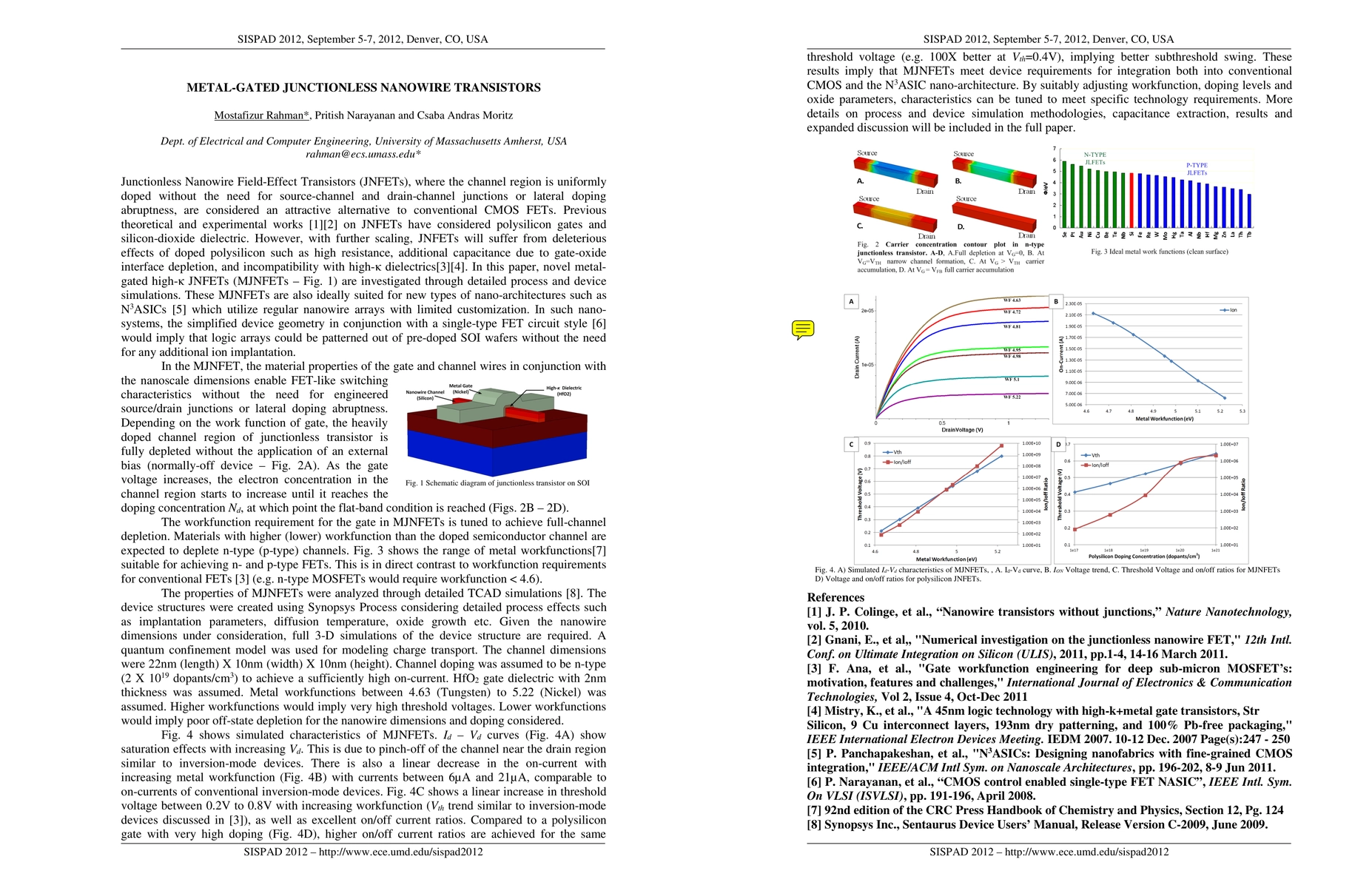
Junctionless Nanowire Field-Effect Transistors (JNFETs), where the channel region is uniformly doped without the need for source-channel and drain-channel junctions or lateral doping abruptness, are considered an attractive alternative to conventional CMOS FETs. Previous theoretical and experimental works [1][2] on JNFETs have considered polysilicon gates and silicon-dioxide dielectric. However, with further scaling, JNFETs will suffer from deleterious effects of doped polysilicon such as high resistance, additional capacitance due to gate-oxide interface depletion, and incompatibility with high-k dielectrics[3][4]. In this paper, novel metal- gated high-k JNFETs are investigated through detailed process and device simulations. These MJNFETs are also ideally suited for new types of nano-architectures such as N3ASICs [5] which utilize regular nanowire arrays with limited customization. In such nano- systems, the simplified device geometry in conjunction with a single-type FET circuit style [6] would imply that logic arrays could be patterned out of pre-doped SOI wafers without the need for any additional ion implantation.
AI Key Findings
Get AI-generated insights about this paper's methodology, results, significance, and more — seven facets brought into focus.
Impact
Paper Details
PDF Preview
Key Terms
Citation Network
Current paper (gray), citations (green), references (blue)
Display is limited for performance on very large graphs.
Discussion 0