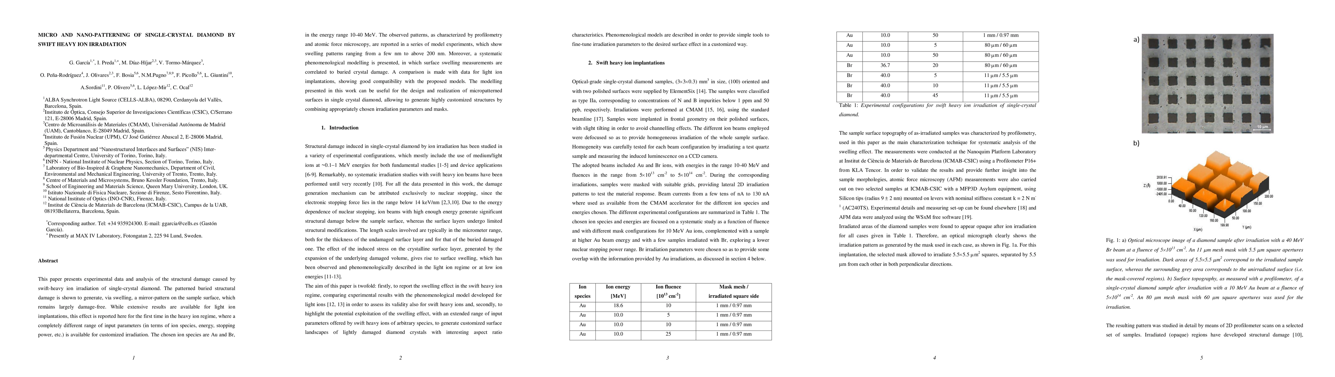
Summary
This paper presents experimental data and analysis of the structural damage caused by swift-heavy ion irradiation of single-crystal diamond. The patterned buried structural damage is shown to generate, via swelling, a mirror-pattern on the sample surface, which remains largely damage-free. While extensive results are available for light ion implantations, this effect is reported here for the first time in the heavy ion regime, where a completely different range of input parameters (in terms of ion species, energy, stopping power, etc.) is available for customized irradiation. The chosen ion species are Au and Br, in the energy range 10-40 MeV. The observed patterns, as characterized by profilometry and atomic force microscopy, are reported in a series of model experiments, which show swelling patterns ranging from a few nm to above 200 nm. Moreover, a systematic phenomenological modelling is presented, in which surface swelling measurements are correlated to buried crystal damage. A comparison is made with data for light ion implantations, showing good compatibility with the proposed models. The modelling presented in this work can be useful for the design and realization of micropatterned surfaces in single crystal diamond, allowing to generate highly customized structures by combining appropriately chosen irradiation parameters and masks.
AI Key Findings
Generated Sep 06, 2025
Methodology
A combination of ion irradiation and thermal annealing techniques were used to create graphitic layers in single-crystal diamond.
Key Results
- The creation of graphitic layers with a thickness of up to 100 nm
- The observation of light guiding in the graphitic layers
- The measurement of electrical conductivity in the graphitic layers
Significance
This research demonstrates the potential for single-crystal diamond to be used as a substrate for optoelectronic devices.
Technical Contribution
A novel method for creating graphitic layers in single-crystal diamond using ion irradiation and thermal annealing.
Novelty
The use of this technique allows for the creation of high-quality, large-area graphitic layers with unique properties
Limitations
- The limited thickness of the graphitic layers
- The difficulty in achieving uniformity across the sample
Future Work
- Investigating the properties of graphitic layers at larger scales
- Developing techniques to improve the uniformity and control of graphitic layer formation
Paper Details
PDF Preview
Key Terms
Citation Network
Current paper (gray), citations (green), references (blue)
Display is limited for performance on very large graphs.
| Title | Authors | Year | Actions |
|---|
Comments (0)