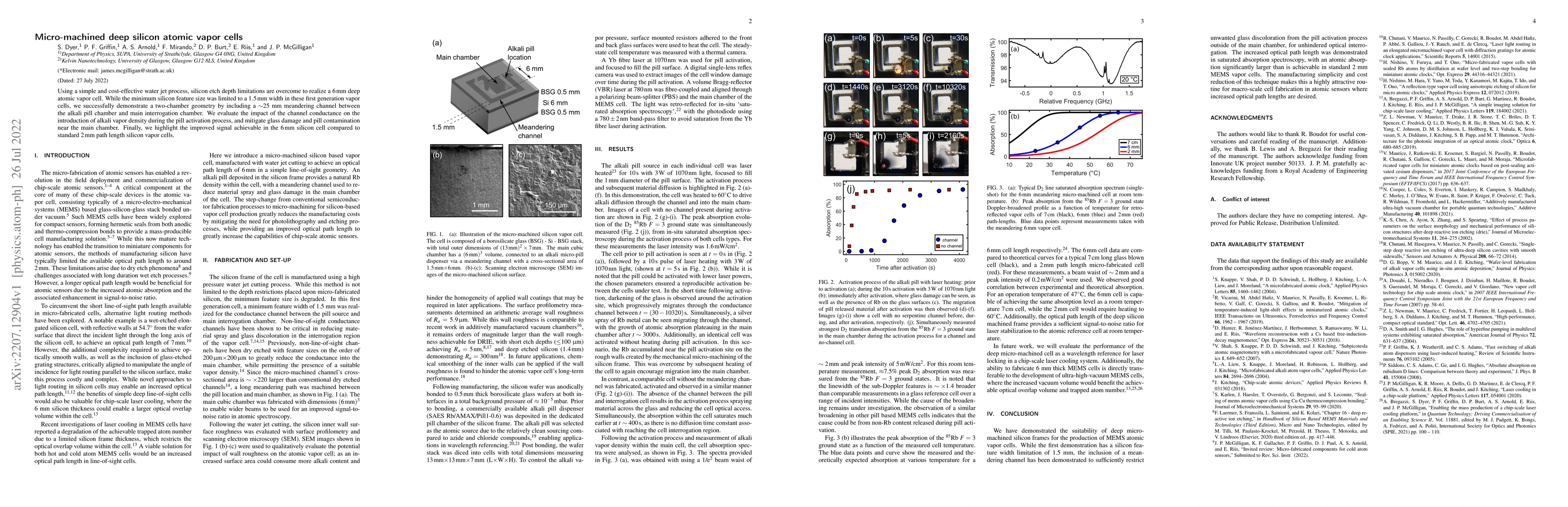
This paper details the development of a micro-machined deep silicon atomic vapor cell using a water jet process, achieving a 6 mm depth and demonstrating a 25 mm meandering channel. The study evaluates the channel's conductance impact on alkali vapor density and highlights improved signal performance compared to standard 2 mm cells.
Using a simple and cost-effective water jet process, silicon etch depth limitations are overcome to realize a $6\,$mm deep atomic vapor cell. While the minimum silicon feature size was limited to a $1.5\,$mm width in these first generation vapor cells, we successfully demonstrate a two-chamber geometry by including a $\sim$25~mm meandering channel between the alkali pill chamber and main interrogation chamber. We evaluate the impact of the channel conductance on the introduction of alkali vapor density during the pill activation process, and mitigate glass damage and pill contamination near the main chamber. Finally, we highlight the improved signal achievable in the $6\,$mm silicon cell compared to standard $2\,$mm path length silicon vapor cells.
Generated Sep 03, 2025
The research utilized a water jet process to overcome silicon etch depth limitations, fabricating a 6 mm deep atomic vapor cell with a minimum feature size of 1.5 mm. The cell features a two-chamber geometry with a meandering channel to introduce alkali vapor density during the pill activation process.
This research presents a cost-effective method to increase the optical path length in atomic vapor cells, which is beneficial for enhancing signal-to-noise ratio in atomic sensors and potentially enabling chip-scale laser cooling applications.
The paper introduces a micro-machined deep silicon atomic vapor cell fabricated using a water jet process, overcoming silicon etch depth limitations and demonstrating a two-chamber geometry with a meandering channel for improved alkali vapor density introduction.
The novelty of this work lies in the simple and cost-effective approach to achieve a longer optical path length in silicon-based atomic vapor cells, which is crucial for enhancing the performance of chip-scale atomic sensors and potentially enabling chip-scale laser cooling.
Current paper (gray), citations (green), references (blue)
Display is limited for performance on very large graphs.
Title | Authors | Year | Actions |
---|
Comments (0)