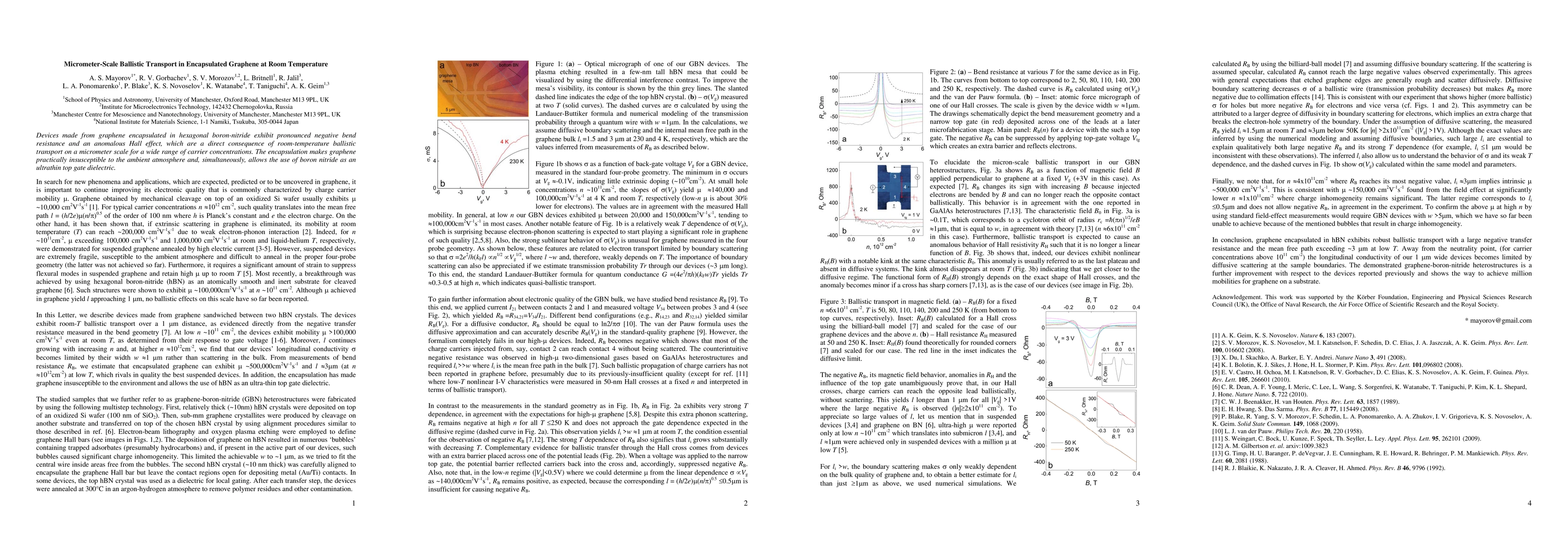
The research utilized a multistep technology to fabricate graphene-boron-nitride (GBN) heterostructures, involving deposition of thick hBN crystals on oxidized Si wafers, transfer of sub-mm graphene crystallites, definition of graphene Hall bars via electron-beam lithography and oxygen plasma etching, and encapsulation of graphene Hall bars with a second hBN crystal. Devices were annealed in an argon-hydrogen atmosphere to remove contaminants.
Publication
Metrics
AI Quick Summary
Summary: Graphene encapsulated in hexagonal boron-nitride demonstrates exceptional room-temperature ballistic transport over micrometer scales, showing pronounced negative bend resistance and an anomalous Hall effect, while remaining protected from ambient atmospheric effects. This encapsulation also enables boron nitride to serve as an effective ultrathin gate dielectric.
Quick Answers
What is "Micrometer-scale ballistic transport in encapsulated graphene at room temperature" about?
Summary: Graphene encapsulated in hexagonal boron-nitride demonstrates exceptional room-temperature ballistic transport over micrometer scales, showing pronounced negative bend resistance and an anomalous Hall effect, while remaining protected from ambient atmospheric effects. This encapsulation also enables boron nitride to serve as an effective ultrathin gate dielectric.
What methodology did the authors use?
The research utilized a multistep technology to fabricate graphene-boron-nitride (GBN) heterostructures, involving deposition of thick hBN crystals on oxidized Si wafers, transfer of sub-mm graphene crystallites, definition of graphene Hall bars via electron-beam lithography and oxygen plasma etching, and encapsulation of graphene Hall bars with a second hBN crystal. Devices were annealed in an argon-hydrogen atmosphere to remove contaminants. More in Methodology →
What are the key results?
Graphene encapsulated in hexagonal boron-nitride exhibits room-temperature ballistic transport over a 1 μm distance. — Devices show mobility μ >100,000 cm2V-1s-1 at low carrier concentrations (~1011 cm-2) and room temperature. More in Key Results →
Why is this work significant?
This research is significant as it demonstrates micrometer-scale ballistic transport in graphene at room temperature, which is crucial for exploring new phenomena and applications in graphene. The findings pave the way for achieving million mobilities for graphene on a substrate, surpassing previous reports of ultra-high mobility at low carrier concentrations. More in Significance →
What are the main limitations?
The study was limited by charge inhomogeneity caused by 'bubbles' containing trapped adsorbates, restricting the achievable width to ~1 μm. — High-mobility devices required annealing, which might not be feasible for all applications. More in Limitations →
Abstract
Devices made from graphene encapsulated in hexagonal boron-nitride exhibit pronounced negative bend resistance and an anomalous Hall effect, which are a direct consequence of room-temperature ballistic transport on a micrometer scale for a wide range of carrier concentrations. The encapsulation makes graphene practically insusceptible to the ambient atmosphere and, simultaneously, allows the use of boron nitride as an ultrathin top gate dielectric.
Key Findings, in focus
Seven facets of this paper, analysed and brought into focus by AI.
This research is significant as it demonstrates micrometer-scale ballistic transport in graphene at room temperature, which is crucial for exploring new phenomena and applications in graphene.
- Graphene encapsulated in hexagonal boron-nitride exhibits room-temperature ballistic transport over a 1 μm distance.
- Devices show mobility μ >100,000 cm2V-1s-1 at low carrier concentrations (~1011 cm-2) and room temperature.
- Mean free path l can reach ~3 μm at low temperatures (≈1012 cm-2) with μ ~500,000 cm2V-1s-1, rivaling high-quality suspended graphene devices.
- Encapsulation makes graphene insusceptible to the ambient atmosphere and allows boron nitride to be used as an ultrathin top gate dielectric.
- Negative bend resistance and anomalous Hall effect are observed, direct consequences of ballistic transport on a micrometer scale.
This research is significant as it demonstrates micrometer-scale ballistic transport in graphene at room temperature, which is crucial for exploring new phenomena and applications in graphene. The findings pave the way for achieving million mobilities for graphene on a substrate, surpassing previous reports of ultra-high mobility at low carrier concentrations.
The paper presents a novel approach to achieving high-quality, ballistic transport in graphene at room temperature by encapsulating it in hexagonal boron-nitride, which protects the graphene from ambient degradation and enables the use of boron nitride as a top gate dielectric.
This work distinguishes itself by demonstrating room-temperature ballistic transport over micrometer scales in graphene encapsulated in hexagonal boron-nitride, surpassing previous reports of ultra-high mobility at low carrier concentrations and in suspended devices.
- The study was limited by charge inhomogeneity caused by 'bubbles' containing trapped adsorbates, restricting the achievable width to ~1 μm.
- High-mobility devices required annealing, which might not be feasible for all applications.
- Investigate methods to minimize charge inhomogeneity caused by adsorbates for larger device dimensions.
- Explore the potential of these GBN heterostructures in various electronic and optoelectronic applications.
Impact
Paper Details
PDF Preview
Key Terms
Citation Network
Current paper (gray), citations (green), references (blue)
Display is limited for performance on very large graphs.
Discussion 0