Publication
Metrics
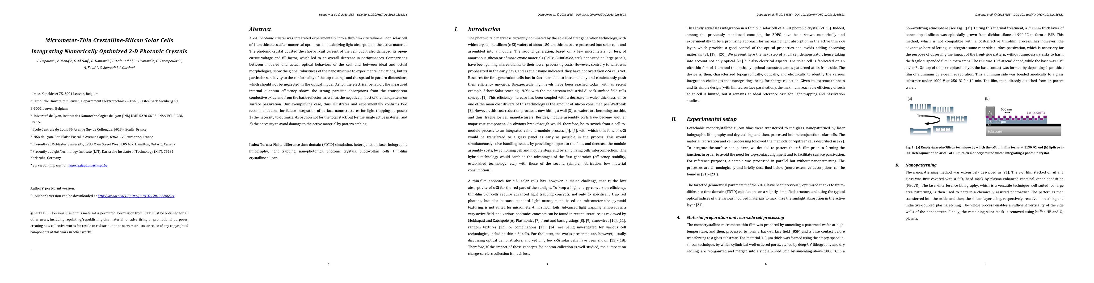
Paper Preview
Abstract
A 2-D photonic crystal was integrated experimentally into a thin-film crystalline-silicon solar cell of 1-{\mu}m thickness, after numerical optimization maximizing light absorption in the active material. The photonic crystal boosted the short-circuit current of the cell, but it also damaged its open-circuit voltage and fill factor, which led to an overall decrease in performances. Comparisons between modeled and actual optical behaviors of the cell, and between ideal and actual morphologies, show the global robustness of the nanostructure to experimental deviations, but its particular sensitivity to the conformality of the top coatings and the spread in pattern dimensions, which should not be neglected in the optical model. As for the electrical behavior, the measured internal quantum efficiency shows the strong parasitic absorptions from the transparent conductive oxide and from the back-reflector, as well as the negative impact of the nanopattern on surface passivation. Our exemplifying case, thus, illustrates and experimentally confirms two recommendations for future integration of surface nanostructures for light trapping purposes: 1) the necessity to optimize absorption not for the total stack but for the single active material, and 2) the necessity to avoid damage to the active material by pattern etching.
AI Key Findings
Get AI-generated insights about this paper's methodology, results, significance, and more — seven facets brought into focus.
Impact
Paper Details
PDF Preview
Key Terms
Citation Network
Current paper (gray), citations (green), references (blue)
Display is limited for performance on very large graphs.
Discussion 0