Microresonator-enhanced, Waveguide-coupled Emission from Silicon Defect Centers for Superconducting Optoelectronic Networks

Source: ArXiv

AI Quick Summary

Summary: This paper discusses advancements in superconducting optoelectronic networks, highlighting recent progress and presenting new findings on cryogenic silicon photonic light sources, which are crucial components for these advanced computing architectures.

Share: Share on X LinkedIn

Summary

Superconducting optoelectronic networks could achieve scales unmatched in hardware-based neuromorphic computing. After summarizing recent progress in this area, we report new results in cryogenic silicon photonic light sources, components central to these architectures.

AI Key Findings

Generated Sep 03, 2025

Methodology

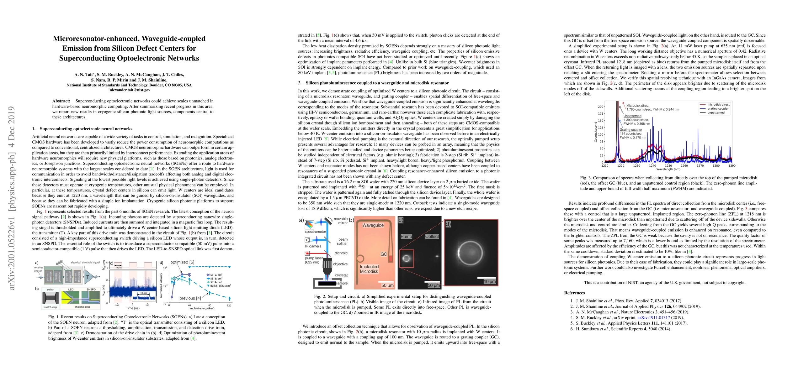
The research utilizes a silicon-on-insulator (SOI) wafer with a 220nm silicon device layer, patterned and implanted with 28Si+ at 25keV and a fluence of 5x10^12/cm^2. The wafer is then encapsulated with a 1.5µm PECVD oxide. W-centers are created by damaging the silicon crystal through ion bombardment and annealing, which are CMOS-compatible at the wafer scale.

Key Results

  • Demonstrated coupling of optimized W-centers to a silicon photonic circuit consisting of a microdisk resonator, waveguide, and grating coupler.
  • Waveguide-coupled emission significantly enhanced at wavelengths corresponding to the resonator's modes.
  • Achieved single-mode waveguide operation at 1220nm, with a waveguide loss of 18.9dB/cm.
  • Observed spatial differentiation between free-space and waveguide-coupled emission, enabling observation of waveguide-coupled photoluminescence (PL).

Significance

This research contributes to the development of large-scale photonics systems by presenting easily fabricated silicon emissive defects, which could play a significant role in superconducting optoelectronic neural networks (SOENs) for hardware-based neuromorphic computing.

Technical Contribution

The paper presents a novel approach to coupling W-center emission to a silicon photonic circuit, enabling spatial differentiation of free-space and waveguide-coupled emission.

Novelty

This work distinguishes itself by utilizing easily fabricated W-centers in silicon-on-insulator substrates, simplifying the process compared to other emitters like III-V semiconductors, germanium, or rare-earths.

Limitations

  • High waveguide loss of 18.9dB/cm compared to other runs, possibly due to a new etch recipe.
  • The study focuses on an optically pumped setup, which may not directly translate to electrical pumping applications.

Future Work

  • Investigate Purcell enhancement, nonlinear phenomena, optical amplifiers, and electrical pumping.
  • Optimize fabrication processes to reduce waveguide losses and improve device performance.

Paper Details

PDF Preview

Download PDF

Key Terms

new results (0.304)
photonic (0.297)
silicon (0.280)
hardware (0.268)
architectures (0.252)
superconducting (0.248)
progress (0.241)
area (0.226)

Citation Network

Current paper (gray), citations (green), references (blue)

Display is limited for performance on very large graphs.

Current Paper
Citations
References
Click to view
Title Authors Year Actions

Comments (0)

This website uses cookies to ensure you get the best experience. Learn more