Microstructure and Elastic Constants of Transition Metal Dichalcogenide Monolayers from Friction and Shear Force Microscopy
Publication
Metrics
Paper Preview
Abstract
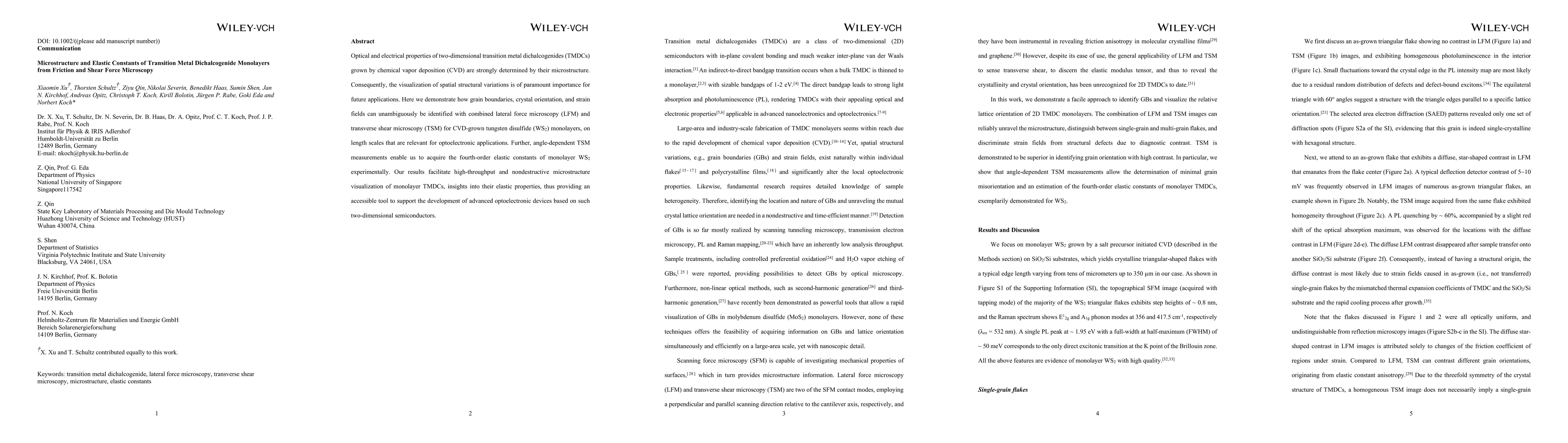
Optical and electrical properties of two-dimensional transition metal dichalcogenides (TMDCs) grown by chemical vapor deposition (CVD) are strongly determined by their microstructure. Consequently, the visualization of spatial structural variations is of paramount importance for future applications. Here we demonstrate how grain boundaries, crystal orientation, and strain fields can unambiguously be identified with combined lateral force microscopy (LFM) and transverse shear microscopy (TSM) for CVD-grown tungsten disulfide (WS2) monolayers, on length scales that are relevant for optoelectronic applications. Further, angle-dependent TSM measurements enable us to acquire the fourth-order elastic constants of monolayer WS2 experimentally. Our results facilitate high-throughput and nondestructive microstructure visualization of monolayer TMDCs, insights into their elastic properties, thus providing an accessible tool to support the development of advanced optoelectronic devices based on such two-dimensional semiconductors.
AI Key Findings
Get AI-generated insights about this paper's methodology, results, significance, and more — seven facets brought into focus.
Impact
Paper Details
Authors
PDF Preview
Key Terms
Citation Network
Current paper (gray), citations (green), references (blue)
Display is limited for performance on very large graphs.
Discussion 0