Mobility and sheet charge in high electron mobility transistor quantum wells from photon-induced transconductance
Publication
Metrics
AI Quick Summary
This paper investigates photon-induced transconductance in high electron mobility transistors, demonstrating that it can yield channel mobility and sheet charge density. The method, applicable to AlGaN/GaN heterostructures, provides an optical alternative to Hall effect and field effect measurements, allowing in-situ transistor mobility assessment.
Paper Preview
Abstract
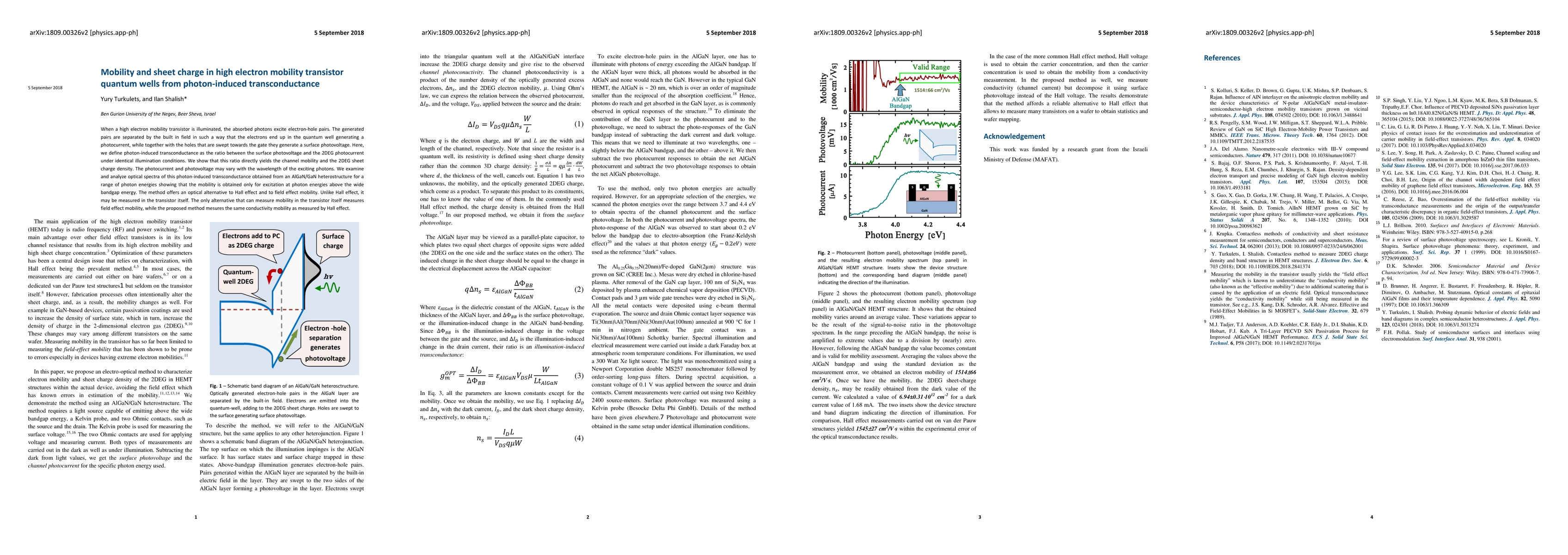
When a high electron mobility transistor is illuminated, the absorbed photons excite electron-hole pairs. The generated pairs are separated by the built in field in such a way that the electrons end up in the quantum well generating a photocurrent, while together with the holes that are swept towards the gate they generate a surface photovoltage. Here, we define photon-induced transconductance as the ratio between the surface photovoltage and the 2DEG photocurrent under identical illumination conditions. We show that this ratio directly yields the channel mobility and the 2DEG sheet charge density. The photocurrent and photovoltage may vary with the wavelength of the exciting photons. We examine and analyze optical spectra of this photon-induced transconductance obtained from an AlGaN/GaN heterostructure for a range of photon energies showing that the mobility is obtained only for excitation at photon energies above the wide bandgap energy. The method offers an optical alternative to Hall effect and to field effect mobility. Unlike Hall effect, it may be measured in the transistor itself. The only alternative that can measure mobility in the transistor itself measures field effect mobility, while the proposed method mesures the same conductivity mobility as measured by Hall effect.
AI Key Findings
Get AI-generated insights about this paper's methodology, results, significance, and more — seven facets brought into focus.
Impact
Paper Details
PDF Preview
Key Terms
Citation Network
Current paper (gray), citations (green), references (blue)
Display is limited for performance on very large graphs.
Discussion 0