Modeling Green's functions measurements with two-tip scanning tunneling microscopy
Publication
Metrics
AI Quick Summary
Researchers propose a new method to measure single-electron Green's functions using two-tip scanning tunneling microscopy, allowing for real-time measurements in 2D systems.
Paper Preview
Abstract
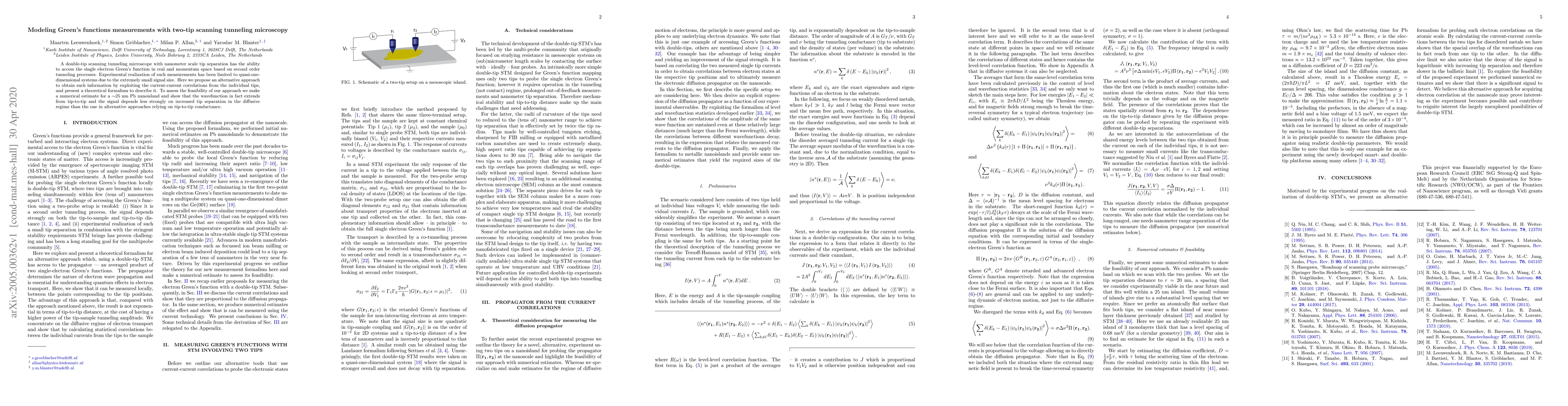
A double-tip scanning tunneling microscope with nanometer scale tip separation has the ability to access the single electron Green's function in real and momentum space based on second order tunneling processes. Experimental realization of such measurements has been limited to quasi-one-dimensional systems due to the extremely small signal size. Here we propose an alternative approach to obtain such information by exploiting the current-current correlations from the individual tips, and present a theoretical formalism to describe it. To assess the feasibility of our approach we make a numerical estimate for a $\sim$ 25 nm Pb nanoisland and show that the wavefunction in fact extends from tip-to-tip and the signal depends less strongly on increased tip separation in the diffusive regime than the one in alternative approaches relying on tip-to-tip conductance.
AI Key Findings
Get AI-generated insights about this paper's methodology, results, significance, and more — seven facets brought into focus.
Impact
Paper Details
Authors
PDF Preview
Key Terms
Citation Network
Current paper (gray), citations (green), references (blue)
Display is limited for performance on very large graphs.
Discussion 0