Quick Summary:

This paper proposes candidate elements for p-type and n-type doping in 2D transition-metal dichalcogenides (TMDs) using modulation doping techniques. First-principles calculations demonstrate successful p-doping in monolayer WSe$_2$ by doping Ni into the HfO$_2$ layer, showing tunable hole concentration for effective electrostatic gate control, which is crucial for TMD-based transistor applications.

Summary

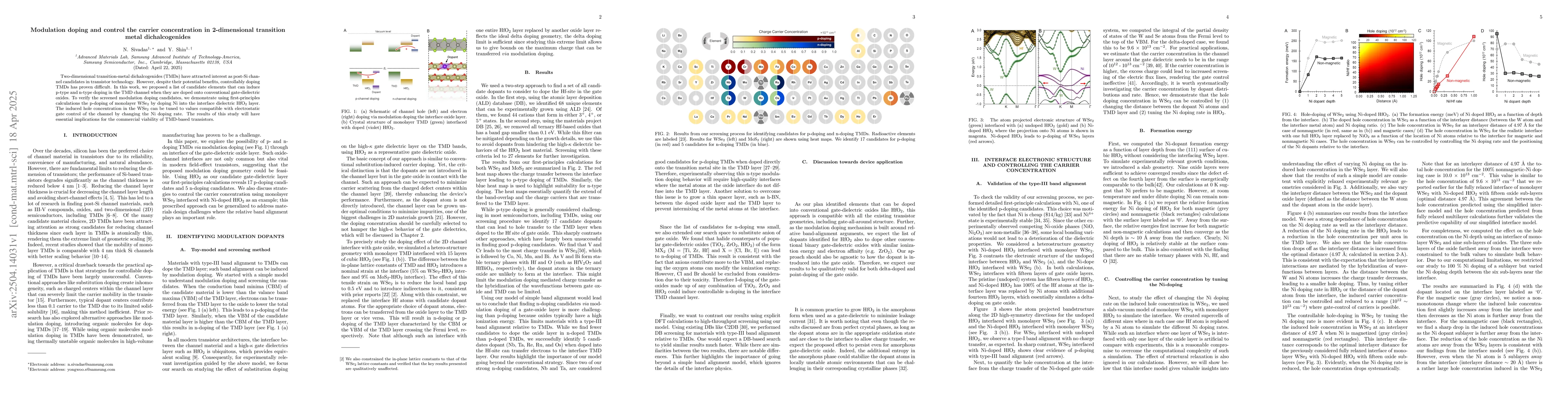
Two-dimensional transition-metal dichalcogenides (TMDs) have attracted interest as post-Si channel candidates in transistor technology. However, despite their potential benefits, controllably doping TMDs has proven difficult. In this work, we proposed a list of candidate elements that can induce p-type and n-type doping in the TMD channel when they are doped onto conventional gate-dielectric oxides. To verify the screened modulation doping candidates, we demonstrate using first-principles calculations the p-doping of monolayer WSe$_2$ by doping Ni int\textbf{}o the interface dielectric HfO$_2$ layer. The induced hole concentration in the WSe$_2$ can be tuned to values compatible with electrostatic gate control of the channel by changing the Ni doping rate. The results of this study will have essential implications for the commercial viability of TMD-based transistors.

AI Key Findings

Generated Jun 09, 2025

Methodology

The research utilized high-throughput screening via DFT calculations to identify elements for p-doping and n-doping in TMDs, proposing modulation doping through conventional gate-dielectric oxides like HfO2.

Key Results

  • Identification of 17 candidates for p-doping (e.g., Ni for WSe2) and 5 for n-doping (halide counterparts of large gate-dielectric oxides like TiO2, ZrO2, HfO2).
  • Demonstration of p-doping of monolayer WSe2 by Ni in HfO2, with induced hole concentration tunable via Ni doping rate for electrostatic gate control.
  • Extension of n-doping search to halide counterparts of common gate-dielectric oxides, suggesting I-doping for controllable n-doping.

Significance

This study has implications for the commercial viability of TMD-based transistors by providing a list of candidate elements for modulation doping, compatible with existing transistor geometries and gate-all-around structures.

Technical Contribution

The paper presents a novel approach to modulation doping TMDs by doping gate-dielectric layers instead of directly creating defects in TMD layers, enabling control over carrier concentration in TMD channels.

Novelty

The work distinguishes itself by proposing a strategy to control carrier concentration in TMDs through modulation doping of gate-dielectric layers, expanding the understanding of doping mechanisms in 2D materials for transistor applications.

Limitations

  • Results are based on perfect crystal phases; practical application in amorphous gate-dielectric oxides requires further investigation.
  • Experimental validation of identified dopants and their effectiveness in real devices is needed.
  • The computational model does not account for all complexities of real interfaces, such as defects and grain boundaries.

Future Work

  • Experimental verification of identified dopants and their performance in TMD-based transistors.
  • Investigation of the proposed doping strategy in other TMD materials and device architectures.
  • Exploration of doping effects in other regions of transistors, such as spacers and contact metals.

Paper Details

PDF Preview

Download PDF

Key Terms

No key terms available for this paper.

No citations found for this paper.

Comments (0)

This website uses cookies to ensure you get the best experience. Learn more