ArxivLens

Quick Summary:

This paper introduces a heterostructure modulation doping method for silicon using aluminium-induced acceptor states in silicon dioxide, overcoming nanoscale doping issues by relocating dopants. It also explores the application of this technique in enhancing hole-selective tunnelling contacts for high-efficiency photovoltaics.

arXiv Id: 1612.03256
Comments: 13 pages, 4 figures
Date Published: 2016-12-13
Date Updated: 2016-12-13

Categories:

Key Terms (TF-IDF):

silicon (0.373)
silicon (0.372)
doping (0.337)
doping (0.322)
nanoscale (0.222)
nanoscale (0.219)
modulation (0.199)
majority (0.195)
modulation (0.192)
majority (0.192)
atoms (0.177)
atoms (0.174)
concept (0.162)
concept (0.160)
fundamental (0.154)
fundamental (0.144)
contacts (0.141)
nanowires (0.140)
contacts (0.134)
semiconductors (0.133)
License: http://arxiv.org/licenses/nonexclusive-distrib/1.0/

Summary:

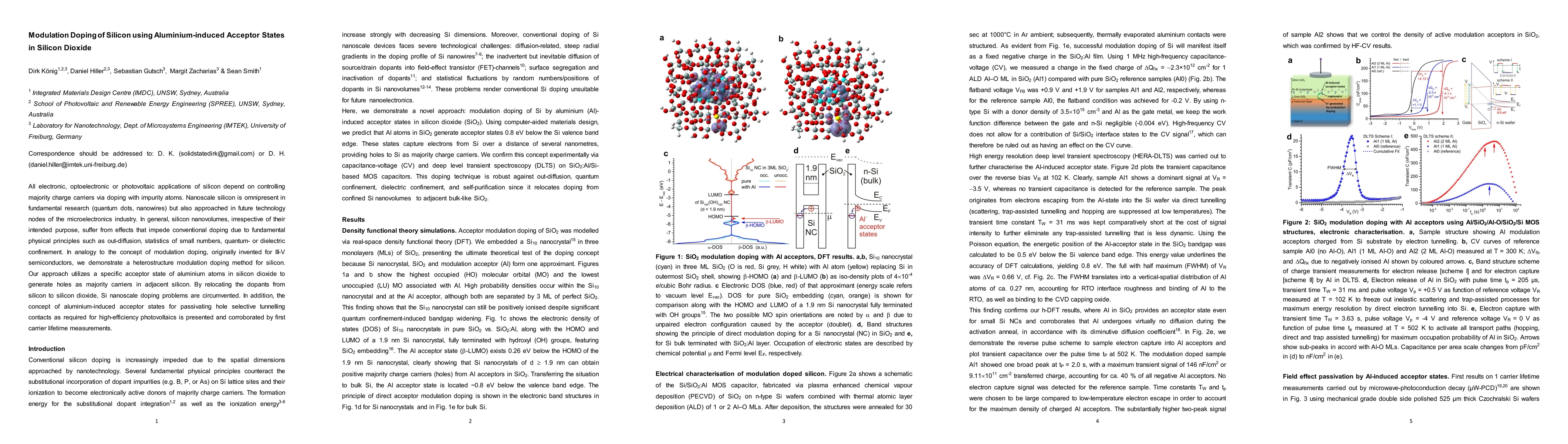
All electronic, optoelectronic or photovoltaic applications of silicon depend on controlling majority charge carriers via doping with impurity atoms. Nanoscale silicon is omnipresent in fundamental research (quantum dots, nanowires) but also approached in future technology nodes of the microelectronics industry. In general, silicon nanovolumes, irrespective of their intended purpose, suffer from effects that impede conventional doping due to fundamental physical principles such as out-diffusion, statistics of small numbers, quantum- or dielectric confinement. In analogy to the concept of modulation doping, originally invented for III-V semiconductors, we demonstrate a heterostructure modulation doping method for silicon. Our approach utilizes a specific acceptor state of aluminium atoms in silicon dioxide to generate holes as majority carriers in adjacent silicon. By relocating the dopants from silicon to silicon dioxide, Si nanoscale doping problems are circumvented. In addition, the concept of aluminium-induced acceptor states for passivating hole selective tunnelling contacts as required for high-efficiency photovoltaics is presented and corroborated by first carrier lifetime measurements.

Citation & Reference Network Visualization

This graph shows how this paper is connected to other research. The current paper is shown in dark gray, papers that cite it are in green, and papers it references are in blue. You can:

Current Paper
Papers citing this work (Citations)
Papers cited by this work (References)

• Hover over any node to see the paper title

• Click a node to view that paper's details

• Drag nodes to rearrange the graph

• Use the zoom controls (bottom right) to zoom in/out

Citations and References

Title Authors Year Actions
Atomic layer deposition of HfO2 as a charge-lean capping layer material for SiO2-modulation acceptor doping of silicon
Somayeh Shams, Ingmar Ratschinski, Daniel Hiller
2025
View Paper
Physical and electrical properties of silica
D. K. Ferry, D. L. Rode
2025
View Paper
Analyzing Carrier Density and Hall Mobility in Impurity‐Free Silicon Virtually Doped by External Defect Placement
Soundarya Nagarajan, Ingmar Ratschinski, S. Schmult, Steffen Wirth, Dirk König, T. Mikolajick, Daniel Hiller, J. Trommer
2024
View Paper
Ultra-shallow p-type doping of silicon by performing atomic layer deposition of Al2O3 thin films onto SiO2/Si.
Salma Khaldi, Prajith Karadan, K. Killi, Clovis Eduardo Mazzotti de Oliveira, R. Yerushalmi
2024
View Paper
Fundamental Origin of Si Surface Defects Caused by Laser Irradiation and Prevention of Suboxide Formation through High Density Ultrathin SiO2
Won Jin Kim, Kee-Ryung Park, Sang Ouk Ryu, B. Kim, Jinhyeong Kwon, Woo-Byoung Kim
2024
View Paper
Hot luminescence of two-dimensional electron hole systems in modulation-doped silicon
F. Heinz, W. Kwapil, S. Glunz
2024
View Paper
Activation of Al2O3 surface passivation of silicon: Separating bulk and surface effects
N.E. Grant, S. Pain, E. Khorani, R. Jefferies, A. Wratten, S. McNab, D. Walker, Y. Han, R. Beanland, R.S. Bonilla, J.D. Murphy
2023
View Paper
Modulation Doping of Silicon Nanowires to Tune the Contact Properties of Nano‐Scale Schottky Barriers
Soundarya Nagarajan, Daniel Hiller, Ingmar Ratschinski, Dirk König, Sean C. Smith, T. Mikolajick, J. Trommer
2023
View Paper
Investigating the Effect of Aluminum Oxide Fixed Charge on Schottky Barrier Height in Molybdenum Oxide-Based Selective Contacts
B. Garland, Benjamin E. Davis, N. Strandwitz
2023
View Paper
Atomic-layer-deposited BOx/Al2O3 stack for crystalline silicon surface passivation
Xinyu Wang, Kun Gao, Dacheng Xu, Kun Li, Chunfang Xing, Xin-li Lou, Zhaojun Su, Xinbo Yang
2023
View Paper
Evaluation of Schottky barrier height at Silicide/Silicon interface of a Silicon Nanowire with Modulation Acceptor Doped Dielectric Shell
Soundarya Nagarajan, D. Hiller, I. Ratschinski, J. Knoch, T. Mikolajick, J. Trommer
2023
View Paper
Application of Si-related Ultrathin (∼1 nm) Films to Crystalline Silicon Solar Cells
K. Ohdaira, H. Nakajima, Yuli Wen, H. Tu
2023
View Paper
SiNx and AlOx Nanolayers in Hole Selective Passivating Contacts for High Efficiency Silicon Solar Cells
S. McNab, Xinya Niu, E. Khorani, A. Wratten, A. Morisset, N. Grant, J. Murphy, P. Altermatt, M. Wright, P. Wilshaw, R. S. Bonilla
2023
View Paper
Controlling the fixed negative charge formation in Si/high- k interfaces
J. Lehtiö, Zahra Sadat Jahanshah Rad, M. Punkkinen, R. Punkkinen, M. Kuzmin, P. Laukkanen, K. Kokko
2022
View Paper
Effect of thermal vacuum nitridation of Si(100) surface via NH3 exposure
M. Ebrahimzadeh, J. Lehtiö, M. Punkkinen, R. Punkkinen, Mikko Miettinen, Z. Rad, M. Kuzmin, P. Laukkanen, K. Kokko
2022
View Paper
Spatially‐Modulated Silicon Interface Energetics Via Hydrogen Plasma‐Assisted Atomic Layer Deposition of Ultrathin Alumina
A. Henning, J. Bartl, Lukas Wolz, Maximilian Christis, F. Rauh, Michele Bissolo, Theresa Grünleitner, J. Eichhorn, P. Zeller, M. Amati, L. Gregoratti, J. Finley, B. Rieger, M. Stutzmann, I. Sharp
2021
View Paper
Excellent surface passivation of germanium by a-Si:H/Al2O3 stacks
W. J. Berghuis, J. Melskens, B. Macco, Roel J. Theeuwes, L. Black, M. Verheijen, W. Kessels
2021
View Paper
Effect of the native oxide on the surface passivation of Si by Al2O3
M. Getz, M. Povoli, E. Monakhov
2021
View Paper
Dopant diffusion through ultrathin AlOx and AlOx/SiOx tunnel layer in TOPCon structure and its impact on the passivation quality on c-Si solar cells
Lu Linna, Yuheng Zeng, Mingdun Liao, Zheng Jingming, Yiran Lin, Mengmeng Feng, Yuyan Zhi, Haiyan He, Ding Wan'er, Chunhui Shou, Ganghua Qin, B. Yan, Jichun Ye
2021
View Paper
The negative fixed charge of atomic layer deposited aluminium oxide—a two-dimensional SiO2/AlO x interface effect
D. Hiller, David Tröger, M. Grube, D. König, T. Mikolajick
2021
View Paper
On the Location of Boron in SiO2‐Embedded Si Nanocrystals—An X‐ray Absorption Spectroscopy and Density Functional Theory Study
D. Hiller, D. König, P. Nagel, M. Merz, S. Schuppler, Sean C. Smith
2021
View Paper
Observation of Si 2p Core‐Level Shift in Si/High‐κ Dielectric Interfaces Containing a Negative Charge
J. Lehtiö, Z. Rad, S. Granroth, M. Yasir, M. Punkkinen, R. Punkkinen, Hannu-Pekka Hedman, J. Rueff, I. T. Rauha, H. Savin, P. Laukkanen, K. Kokko
2021
View Paper
Material combination of Tunnel-SiO2 with a (sub-)Monolayer of ALD-AlOx on silicon offering a highly passivating hole selective contact
D. Hiller, P. Hönicke, D. König
2020
View Paper
Influence of layer thickness on passivation properties in SiOx/Al2O3 stacks
A. ek, C. Reichel, A. Richter, J. Benick
2020
View Paper
Non-equilibrium dynamics, materials and structures for hot carrier solar cells: a detailed review
Dirk König, Yao Yao, B. Puthen-Veettil, J. C. Smith
2020
View Paper
Electronic Structure Shift of Deeply Nanoscale Silicon by SiO2 versus Si3N4 Embedding as an Alternative to Impurity Doping
D. König, N. Wilck, D. Hiller, B. Berghoff, A. Meledin, G. Di Santo, L. Petaccia, J. Mayer, Sean C. Smith, J. Knoch
2019
View Paper
N-Doping at the Sub-Nanoscale: Dielectric and Magnetic Response of Neutral Phosphorus-Doped Tin Clusters.
Martin Gleditzsch, T. Fuchs, R. Schäfer
2019
View Paper
Deactivation of silicon surface states by Al-induced acceptor states from Al–O monolayers in SiO2
D. Hiller, P. Jordan, K. Ding, M. Pomaska, T. Mikolajick, D. König
2019
View Paper
SiO2 Modulation Doping for Si : Acceptor Candidates
D. König, D. Hiller, Sean C. Smith
2018
View Paper
Room-temperature single dopant atom quantum dot transistors in silicon, formed by field-emission scanning probe lithography
Z. Durrani, Mervyn E. Jones, Faris Abualnaja, Chen Wang, M. Kaestner, S. Lenk, C. Lenk, I. Rangelow, A. Andreev
2018
View Paper
Intrinsic ultrasmall nanoscale silicon turns n-/p-type with SiO2/Si3N4-coating
D. König, D. Hiller, N. Wilck, B. Berghoff, M. Müller, S. Thakur, G. Di Santo, L. Petaccia, J. Mayer, Sean C. Smith, J. Knoch
2018
View Paper
Synthesis, optical properties and theoretical modelling of discrete emitting states in doped silicon nanocrystals for bioimaging.
B. F. P. McVey, Dirk König, Xiaoyu Cheng, Peter B O'Mara, Prasenjit Seal, Xin Tan, H. Tahini, Sean C. Smith, J. Gooding, R. Tilley
2018
View Paper
Structural Properties of Al-O Monolayers in SiO2 on Silicon and the Maximization of Their Negative Fixed Charge Density.
D. Hiller, J. Göttlicher, R. Steininger, T. Huthwelker, J. Julin, F. Munnik, M. Wahl, W. Bock, B. Schoenaers, A. Stesmans, Dirk Koenig
2018
View Paper
Absence of free carriers in silicon nanocrystals grown from phosphorus- and boron-doped silicon-rich oxide and oxynitride
D. Hiller, J. López-Vidrier, K. Nomoto, M. Wahl, W. Bock, Tomáš Chlouba, F. Trojánek, S. Gutsch, M. Zacharias, D. König, P. Malý, M. Kopnarski
2018
View Paper
Boron-Incorporating Silicon Nanocrystals Embedded in SiO2: Absence of Free Carriers vs. B-Induced Defects
D. Hiller, J. López-Vidrier, S. Gutsch, M. Zacharias, M. Wahl, W. Bock, A. Brodyanski, M. Kopnarski, K. Nomoto, J. Valenta, D. König
2017
View Paper
Defect-Induced Luminescence Quenching vs. Charge Carrier Generation of Phosphorus Incorporated in Silicon Nanocrystals as Function of Size
D. Hiller, J. López-Vidrier, S. Gutsch, M. Zacharias, K. Nomoto, D. König
2017
View Paper
Alternative dielectrics for hole selective passivating contacts and the influence of nanolayer built-in charge
S. McNab, Mingzhe Yu, Isabel Al-Dhahir, E. Khorani, Tasmiat Rahman, S. Boden, P. Altermatt, P. Wilshaw, R. S. Bonilla
2022
View Paper

Comments (0)

This website uses cookies to ensure you get the best experience. Learn more