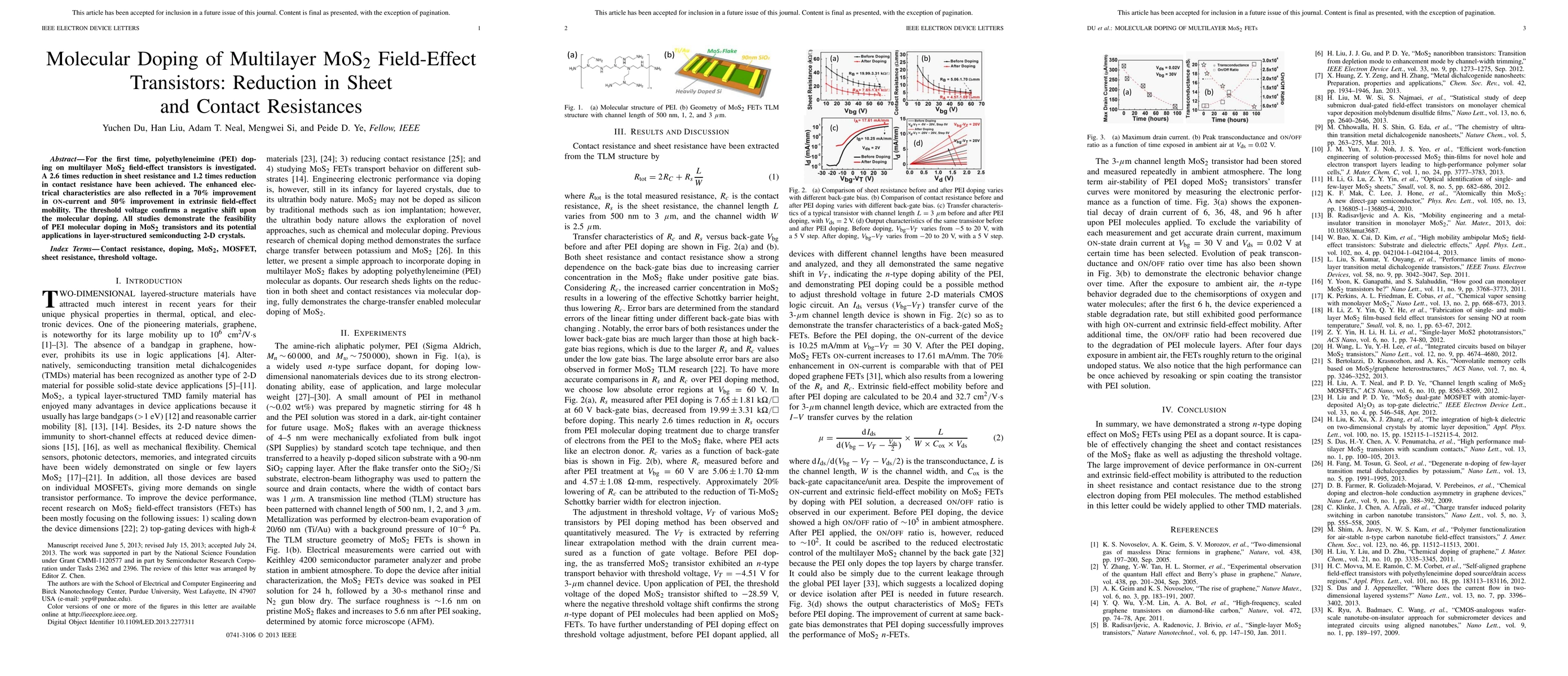
Researchers achieved significant improvements in MoS2 transistors through molecular doping with polyethyleneimine, reducing sheet resistance by 2.6 times and extrinsic mobility by 50%. This breakthrough demonstrates the feasibility of PEI doping for potential applications in 2D semiconducting crystals.
For the first time, polyethyleneimine (PEI) doping on multilayer MoS2 field-effect transistors are investigated. A 2.6 times reduction in sheet resistance, and 1.2 times reduction in contact resistance have been achieved. The enhanced electrical characteristics are also reflected in a 70% improvement in ON current, and 50% improvement in extrinsic field-effect mobility. The threshold voltage also confirms a negative shift upon the molecular doping. All studies demonstrate the feasibility of PEI molecular doping in MoS2 transistors, and its potential applications in layer-structured semiconducting 2D crystals.
Get AI-generated insights about this paper's methodology, results, and significance.
Current paper (gray), citations (green), references (blue)
Title | Authors | Year | Actions |
---|---|---|---|
Contact engineering for two-dimensional van der Waals semiconductors
|
Jiachen Tang, Shuaixing Li, Li Zhan, Songlin Li
|
2024
|
View Paper |
UV-Ozone-Assisted Solution-Processed High-k ZrO₂for MoS₂ Field-Effect Transistors
|
Yepeng Shi, Guoxia Liu, Xiaomin Wu, Chengjie Zhou, Chengzhi Yang, Zhenyu Yang, F. Shan
|
2024
|
View Paper |
High-Photosensitivity WSe2 Phototransistor with Electrically Self-Isolated C8-BTBT as a Light Absorption Layer
|
JaeWan Park, Seongin Hong
|
2024
|
View Paper |
Simulation studies on MoS2 (n)/a-Si:H (i)/c-Si (p)/MoO3 heterojunction solar cells using one sided short diode approximation
|
H. Deka, A. K. Sunaniya, P. Agarwal
|
2023
|
View Paper |
Schottky barrier height engineering on MoS2 field-effect transistors using a polymer surface modifier on a contact electrode
|
D. Choi, Jeehoon Jeon, Taegyun Park, B. Ju, Ki-Young Lee
|
2023
|
View Paper |
Combination of Polymer Gate Dielectric and Two-Dimensional Semiconductor for Emerging Field-Effect Transistors
|
Junhwan Choi, Hocheon Yoo
|
2023
|
View Paper |
Electrical monitoring of organic crystal phase transition using MoS2 field effect transistor
|
ilan Boulet, S. Pascal, F. Bedu, Igor Ozerov, A. Ranguis, Thomas Leoni, Conrad Becker, L. Masson, A. Matković, C. Teichert, O. Siri, C. Attaccalite, J. Huntzinger, M. Paillet, A. Zahab, R. Parret
|
2023
|
View Paper |
Controlled synthesis of ultrathin metallic MoO_2 nanosheets for van der Waals contact
|
Lizhen Fang, Huawei Liu, Wen Guan, B. Zheng, Jieyuan Liang, Tinghao Wang, Xiaoli Zhu, Siyu Li, Dong Li, A. Pan
|
2022
|
View Paper |
Strong photodetection enhancement of quasi-2D transistor through defect engineering
|
Chuanyang Cai, Pengfei Hou, P. Zhou, Bo Li
|
2022
|
View Paper |
Realization of cost-effective and high-performance solar-blind ultraviolet photodetectors based on amorphous Ga2O3 prepared at room temperature
|
Yifei Wang, Yixin Xue, Jie Su, Zhenhua Lin, Jincheng Zhang, Jingjing Chang, Yue Hao
|
2022
|
View Paper |
Improvement of Visible Photodetection of Chemical Vapor Deposition-Grown MoS2 Devices via Graphene/Au Contacts
|
Yeongsik Hwa, Sang‐Soo Chee
|
2022
|
View Paper |
Tunable, stable, and reversible n-type doping of MoS2 via thermal treatment in N-methyl-2-pyrrolidone
|
Hyeyeon Sunwoo, W. Choi
|
2022
|
View Paper |
MoS2 Transistors with Low Schottky Barrier Contact by Optimizing the Interfacial Layer Thickness
|
Jinbing Cheng, Junbao He, C. Pu, Congbin Liu, Xiaoyu Huang, Deyang Zhang, Hailong Yan, P. Chu
|
2022
|
View Paper |
Positive Seebeck coefficient of niobium-doped MoS2 film deposited by sputtering and activated by sulfur vapor annealing
|
Taiga Horiguchi, T. Hamada, M. Hamada, I. Muneta, K. Kakushima, K. Tsutsui, T. Tatsumi, S. Tomiya, H. Wakabayashi
|
2022
|
View Paper |
Synergistic hole-doping on ultrathin MoTe2 for highly stable unipolar field-effect transistor
|
Phuong Huyen Nguyen, Duc Hieu Nguyen, Hyojung Kim, Hyung Mo Jeong, Hye Min Oh, Mun Seok Jeong
|
2022
|
View Paper |
2D-Mo3S4 phase as promising contact for MoS2
|
E. Sukhanova, A. Kvashnin, L. A. Bereznikova, H. Zakaryan, M. A. Aghamalyan, D. Kvashnin, Z. I. Popov
|
2022
|
View Paper |
Fabrication of p-MoS2/n-Si heterojunction by AuCl3 treatment for IR detection
|
D. Pradhan, A. Gartia, Kiran K. Sahoo, S. Ghosh, J. Kar
|
2022
|
View Paper |
Growth of highly conducting MoS2-xNx thin films with enhanced 1T' phase by pulsed laser deposition and exploration of their nanogenerator application
|
Swati Parmar, Neetu Prajesh, M. Wable, R. Choudhary, S. Gosavi, R. Boomishankar, S. Ogale
|
2022
|
View Paper |
Numerical investigation of graphene and 2D‐MoS2 facilitated perovskite/silicon “p‐i‐n” structure for solar cell application
|
Chandra Kamal Borah, Sanjeev Kumar
|
2022
|
View Paper |
Large difference of doping behavior of tetracyanoquinodimethane (TCNQ) and 2,3,5,6-Tetrafluoro-7,7,8,8- tetracyanoquinodimethane (F4-TCNQ) on field effect transistor with channel of atomic layer MoS2
|
Hiroki Waizumi, Muhammad Shamim Al Mamun, T. Takaoka, Md Iftekharul Alam, Yudai Tanaka, A. Ando, Zhipeng Wang, R. Arafune, T. Komeda
|
2022
|
View Paper |
Encapsulation strategies on 2D materials for field effect transistors and photodetectors
|
Wenjuan Huang, Yue Zhang, Mengting Song, Bugao Wang, Huayi Hou, Xiaozong Hu, Xiangbai Chen, T. Zhai
|
2021
|
View Paper |
Metal–semiconductor interface engineering in layered 2D materials for device applications
|
Monika Moun, Rajendra Singh
|
2021
|
View Paper |
p-/n-Type modulation of 2D transition metal dichalcogenides for electronic and optoelectronic devices
|
Songyu Li, Yang Ma, Nabonswende Aida Nadege Ouedraogo, Fa-min Liu, Congya You, Wenjie Deng, Yongzhe Zhang
|
2021
|
View Paper |
Fabrication of Large-Area Molybdenum Disulfide Device Arrays Using Graphene/Ti Contacts
|
M. Son, Jaewon Jang, Dong Chul Kim, Seunghyup Lee, Hyo‐Soon Shin, M. Ham, Sang‐Soo Chee
|
2021
|
View Paper |
Non-invasively improving the Schottky barrier of MoS2/metal contacts by inserting a SiC layer.
|
Qinglong Fang, Xumei Zhao, Lin Yuan, Boyu Wang, C. Xia, F. Ma
|
2021
|
View Paper |
Fermi-level depinning of 2D transition metal dichalcogenide transistors
|
Ruoting Chen, Guanglong Ding, Ye Zhou, Su‐Ting Han
|
2021
|
View Paper |
Molecular Doping of 2D Indium Selenide for Ultrahigh Performance and Low‐Power Consumption Broadband Photodetectors
|
Ye Wang, Hanlin Wang, S. M. Gali, Nicholas Turetta, Yifan Yao, Can Wang, Yusheng Chen, D. Beljonne, P. Samorí
|
2021
|
View Paper |
Recent Advances in Electrical Doping of 2D Semiconductor Materials: Methods, Analyses, and Applications
|
Hocheon Yoo, K. Heo, Md. Hasan Raza Ansari, Seongjae Cho
|
2021
|
View Paper |
MoS2 doping by atomic layer deposition of high-k dielectrics using alcohol as process oxidants
|
Whang Je Woo, Seung Gi Seo, Taewook Nam, Youngjun Kim, Donghyun Kim, J. Song, I. Oh, J. Lim, Hyung-Jun Kim
|
2021
|
View Paper |
Heteroatoms/molecules to tune the properties of 2D materials
|
Xingguo Wang, Lingjia Meng, Bixuan Li, Y. Gong
|
2021
|
View Paper |
N-type and p-type molecular doping on monolayer MoS2
|
Ong Kim Le, V. Chihaia, Vo Van On, D. Son
|
2021
|
View Paper |
Monolayer transition-metal dichalcogenides with polyethyleneimine adsorption
|
Vo Khuong Dien, Ong Kim Le, V. Chihaia, M. Pham-Ho, D. Son
|
2021
|
View Paper |
Recent progress in the development of backplane thin film transistors for information displays
|
Dongseob Ji, Jisu Jang, Joonhyung Park, Dasol Kim, Y. Rim, D. Hwang, Yong‐Young Noh
|
2020
|
View Paper |
The effect of the dopant’s reactivity for high-performance 2D MoS2 thin-film transistor
|
Hanleem Lee, Sora Bak, Joosung Kim, Hyoyoung Lee
|
2020
|
View Paper |
Air stable and reversible n-type surface functionalization of MoS2 monolayer using Arg and Lys amino acids
|
Mengge Li, Jiadong Yao, Yali Liu, Xiaoxiang Wu, Yingxia Yu, Boran Xing, Xiaoyuan Yan, Wenxuan Guo, M. Tan, J. Sha, Yewu Wang
|
2020
|
View Paper |
Characteristics of Cl-doped MoS2 field-effect transistors
|
Tae Young Kim, Yoonsok Kim, E. Kim
|
2020
|
View Paper |
Surface charge transfer doping for two-dimensional semiconductor-based electronic and optoelectronic devices
|
Yanan Wang, Yue Zheng, Cheng Han, Wei Chen
|
2020
|
View Paper |
The prospective application of a graphene/MoS2 heterostructure in Si-HIT solar cells for higher efficiency
|
Chandra Kamal Borah, P. Tyagi, Sanjeev Kumar
|
2020
|
View Paper |
Doping-free complementary WSe2 circuit via van der Waals metal integration
|
Lingan Kong, Xiaodong Zhang, Quanyang Tao, Mingliang Zhang, Weiqi Dang, Zhiwei Li, Li-ping Feng, L. Liao, X. Duan, Yuan Liu
|
2020
|
View Paper |
Interface engineering of two-dimensional transition metal dichalcogenides towards next-generation electronic devices: recent advances and challenges.
|
W. Liao, Siwen Zhao, Feng Li, Cong Wang, Yanqi Ge, Huide Wang, Shibo Wang, Han Zhang
|
2020
|
View Paper |
Hybrid Polymer/Metal Oxide Thin Films for High Performance, Flexible Transistors
|
J. Jeong, Hye suk Hwang, Dalsu Choi, Byung Chol Ma, Jaehan Jung, Mincheol Chang
|
2020
|
View Paper |
Electron irradiation of multilayer PdSe2 field effect transistors
|
A. Di Bartolomeo, F. Urban, A. Pelella, A. Grillo, M. Passacantando, Xiaowei Liu, F. Giubileo
|
2020
|
View Paper |
Polymeric Electron-Selective Contact for Crystalline Silicon Solar Cells with an Efficiency Exceeding 19%
|
Wenbo Ji, T. Allen, Xinbo Yang, Guosong Zeng, Stefaan De Wolf, A. Javey
|
2020
|
View Paper |
2D semiconducting materials for electronic and optoelectronic applications: potential and challenge
|
Sojung Kang, Donghun Lee, Jonghun Kim, A. Capasso, H. Kang, Jin-Woo Park, Chul-Ho Lee, Gwan‐Hyoung Lee
|
2020
|
View Paper |
Tunable Optoelectronic Properties of WS2 by Local Strain Engineering and Folding
|
A. Khan, Teng Lu, Wendi Ma, Yuerui Lu, Yun Liu
|
2020
|
View Paper |
Effect of Al2O3 deposition on carrier mobility and ambient stability of few-layer MoS2 field effect transistors
|
Jong Hwa Ryu, Y. You, Sung Won Kim, Jungpyo Hong, Jeonghyeon Na, S. Jhang
|
2020
|
View Paper |
Electronic and optical properties of monolayer MoS2 under the influence of polyethyleneimine adsorption and pressure
|
Ong Kim Le, V. Chihaia, M. Pham-Ho, D. Son
|
2020
|
View Paper |
Nanotip Contacts for Electric Transport and Field Emission Characterization of Ultrathin MoS2 Flakes
|
L. Iemmo, F. Urban, F. Giubileo, M. Passacantando, A. Di Bartolomeo
|
2020
|
View Paper |
Investigation on 2D Transition Metal Chalcogenide Using Angular-Resolved Photoelectron Spectroscopy
|
Soohyung Park
|
2019
|
View Paper |
A high-pressure enhanced coupling effect between graphene electrical contacts and two-dimensional materials thereby improving the performance of their constituent FET devices
|
Lijie Zhou, Chuanyang Ge, Huihui Yang, Yi Sun, Jia Zhang
|
2019
|
View Paper |
Work function of GaAs(hkl) and its modification using PEI: mechanisms and substrate dependence.
|
S. D. Seddon, C. Benjamin, J. I. Bryant, C. Burrows, M. Walker, Graham Matheson, J. Herranz, L. Geelhaar, G. Bell
|
2019
|
View Paper |
Tailoring the electrical properties of MoTe2 field effect transistor via chemical doping
|
M. W. Iqbal, A. Amin, M. A. Kamran, H. Ateeq, E. Elahi, G. Hussain, S. Azam, S. Aftab, Thamer Alharbi, A. Majid
|
2019
|
View Paper |
Monolayer MoS2 field effect transistor with low Schottky barrier height with ferromagnetic metal contacts
|
Sachin Gupta, F. Rortais, R. Ohshima, Y. Ando, T. Endo, Y. Miyata, M. Shiraishi
|
2019
|
View Paper |
Demonstration of the key substrate-dependent charge transfer mechanisms between monolayer MoS2 and molecular dopants
|
Soohyung Park, T. Schultz, Xiaomin Xu, Berthold Wegner, A. Aljarb, A. Han, Lain‐Jong Li, V. Tung, P. Amsalem, N. Koch
|
2019
|
View Paper |
Synergistic additive-mediated CVD growth and chemical modification of 2D materials.
|
Jizhou Jiang, Neng Li, Jing Zou, Xing Zhou, G. Eda, Qingfu Zhang, Hua Zhang, Lain‐Jong Li, T. Zhai, A. Wee
|
2019
|
View Paper |
Improvement of the Bias Stress Stability in 2D MoS2 and WS2 Transistors with a TiO2 Interfacial Layer
|
Woojin Park, Y. Pak, Hye Yeon Jang, J. Nam, Tae Hyeon Kim, Seyoung Oh, S. Choi, Yonghun Kim, B. Cho
|
2019
|
View Paper |
MoS2 dual-gate transistors with electrostatically doped contacts
|
Fuyou Liao, Y. Sheng, Zhongxun Guo, Hongwei Tang, Yin Wang, Lingyi Zong, Xinyu Chen, A. Riaud, Jiahe Zhu, Yufeng Xie, Lin Chen, Hao Zhu, Qingqing Sun, P. Zhou, Xiangwei Jiang, J. Wan, W. Bao, David-Wei Zhang
|
2019
|
View Paper |
Recent Advances in Interface Engineering of Transition Metal Dichalcogenides with Organic Molecules and Polymers.
|
Kyungjun Cho, Jinsu Pak, Seungjun Chung, Takhee Lee
|
2019
|
View Paper |
Convection‐Flow‐Assisted Preparation of a Strong Electron Dopant, Benzyl Viologen, for Surface‐Charge Transfer Doping of Molybdenum Disulfide
|
Keigo Matsuyama, A. Fukui, K. Miura, H. Ichimiya, Y. Aoki, Yuki Yamada, A. Ashida, T. Yoshimura, N. Fujimura, D. Kiriya
|
2019
|
View Paper |
Nanoscale electronic devices based on transition metal dichalcogenides
|
Wenjuan Zhu, T. Low, Han Wang, P. Ye, X. Duan
|
2019
|
View Paper |
Selectively Metallized 2D Materials for Simple Logic Devices.
|
A. Dathbun, Youngchan Kim, Yongsuk Choi, Jia Sun, Seongchan Kim, B. Kang, Moon-Sung Kang, D. Hwang, Sungjoo Lee, Changgu Lee, J. Cho
|
2019
|
View Paper |
Reproducible Performance Improvements to Monolayer MoS2 Transistors through Exposed Material Forming Gas Annealing.
|
Nicholas B. Guros, S. Le, Siyuan Zhang, B. Sperling, Jeffery B. Klauda, C. Richter, Arvind K. Balijepalli
|
2019
|
View Paper |
Chalcogen-Assisted Enhanced Atomic Orbital Interaction at TMD–Metal Interface and Sulfur Passivation for Overall Performance Boost of 2-D TMD FETs
|
.. Ansh, M. Shrivastava, J. Kumar, G. Sheoran, H. B. Variar, Ravi K. Mishra, Hemanjaneyulu Kuruva, A. Meersha, A. Mishra, S. Raghavan
|
2019
|
View Paper |
H2S assisted contact engineering: a universal approach to enhance hole conduction in all TMD Field-Effect Transistors and achieve ambipolar CVD MoS2 Transistors.
|
Ansh, J. Kumar, Ravi K. Mishra, S. Raghavan, M. Shrivastava
|
2019
|
View Paper |
Controlled p-type substitutional doping in large-area monolayer WSe2 crystals grown by chemical vapor deposition.
|
S. Pandey, Hussain Alsalman, Javad G. Azadani, Nezhueyotl Izquierdo, T. Low, S. Campbell
|
2018
|
View Paper |
Electrical contacts to two-dimensional transition-metal dichalcogenides
|
Shuxian Wang, Zhihao Yu, Xinran Wang
|
2018
|
View Paper |
Two-dimensional Electronics: From Material Synthesis to Device Applications
|
Shan Zheng
|
2018
|
View Paper |
Lowering the Schottky Barrier Height by Graphene/Ag Electrodes for High‐Mobility MoS2 Field‐Effect Transistors
|
Sang‐Soo Chee, D. Seo, H. Kim, Hanbyeol Jang, Seungmin Lee, S. Moon, Kyu Hyoung Lee, Sung Wng Kim, Hyunyong Choi, M. Ham
|
2018
|
View Paper |
Air and Water‐Stable n‐Type Doping and Encapsulation of Flexible MoS2 Devices with SU8
|
Yen‐Cheng Kung, N. Hosseini, D. Dumcenco, G. Fantner, A. Kis
|
2018
|
View Paper |
Chromium–doped MoS2 “inorganic fullerene” nanoparticles prepared by topotactic reaction from oxosalt precursor
|
C. Oumahi, P. Afanasiev
|
2018
|
View Paper |
Research progress and challenges of two dimensional MoS2 field effect transistors
|
N. Divya Bharathi, K. Sivasankaran
|
2018
|
View Paper |
Charge carrier injection and transport engineering in two-dimensional transition metal dichalcogenides
|
J. D. Durán Retamal, Dharmaraj Periyanagounder, Jr-jian Ke, M. Tsai, Jr-hau He
|
2018
|
View Paper |
Molecular chemistry approaches for tuning the properties of two-dimensional transition metal dichalcogenides.
|
Simone Bertolazzi, M. Gobbi, Yuda Zhao, C. Backes, P. Samorí
|
2018
|
View Paper |
Progress in Contact, Doping and Mobility Engineering of MoS2: An Atomically Thin 2D Semiconductor
|
A. Rai, Hema C. P. Movva, A. Roy, D. Taneja, Sayema Chowdhury, S. Banerjee
|
2018
|
View Paper |
Controllable, Wide‐Ranging n‐Doping and p‐Doping of Monolayer Group 6 Transition‐Metal Disulfides and Diselenides
|
Siyuan Zhang, H. Hill, K. Moudgil, C. Richter, A. H. Hight Walker, S. Barlow, S. Marder, C. Hacker, S. Pookpanratana
|
2018
|
View Paper |
Field effect properties of single-layer MoS2(1−x)Se2x nanosheets produced by a one-step CVD process
|
Dengxuan Tang, Fang Wang, Baijun Zhang, Yi Li, Yue Li, Yulin Feng, Yemei Han, Jun Ma, Tianling Ren, Kailiang Zhang
|
2018
|
View Paper |
Ohmic contact between titanium and sputtered MoS2 films achieved by forming-gas annealing
|
Mayato Toyama, T. Ohashi, K. Matsuura, J. Shimizu, I. Muneta, K. Kakushima, K. Tsutsui, H. Wakabayashi
|
2018
|
View Paper |
Reaction of N,N'-dimethylformamide and divalent viologen molecule to generate an organic dopant for molybdenum disulfide
|
A. Fukui, K. Miura, H. Ichimiya, A. Tsurusaki, K. Kariya, T. Yoshimura, A. Ashida, N. Fujimura, D. Kiriya
|
2018
|
View Paper |
Controllable doping and anisotropic properties of two-dimensional materials
|
K. Xu
|
2018
|
View Paper |
Two-dimensional transition metal dichalcogenides: interface and defect engineering.
|
Zehua Hu, Zhangting Wu, Cheng Han, Jun He, Zhenhua Ni, Wei Chen
|
2018
|
View Paper |
The organic-2D transition metal dichalcogenide heterointerface.
|
Y. Huang, Y. Zheng, Zhibo Song, D. Chi, A. Wee, S. Y. Quek
|
2018
|
View Paper |
High performance solution processed oxide thin-film transistors with inkjet printed Ag source–drain electrodes
|
Liam Gillan, J. Leppäniemi, K. Eiroma, H. Majumdar, A. Alastalo
|
2018
|
View Paper |
Direct Covalent Chemical Functionalization of Unmodified Two-Dimensional Molybdenum Disulfide
|
Ximo S. Chu, A. Yousaf, Duo O. Li, A. Tang, Abhishek Debnath, D. Ma, A. Green, E. Santos, Qing Hua Wang
|
2018
|
View Paper |
Effect of Dielectric Interface on the Performance of MoS2 Transistors.
|
Xuefei Li, Xiong Xiong, Tiaoyang Li, Sichao Li, Zhenfeng Zhang, Yanqing Wu
|
2017
|
View Paper |
Stable MoS2 Field‐Effect Transistors Using TiO2 Interfacial Layer at Metal/MoS2 Contact
|
Woojin Park, J. Min, S. Shaikh, M. Hussain
|
2017
|
View Paper |
Combining 2D inorganic semiconductors and organic polymers at the frontier of the hard–soft materials interface
|
A. Ramasubramaniam, Ryan C. Selhorst, Hadas Alon, M. Barnes, T. Emrick, D. Naveh
|
2017
|
View Paper |
Promising Approach for High-Performance MoS2 Nanodevice: Doping the BN Buffer Layer to Eliminate the Schottky Barriers.
|
J. Su, Li-ping Feng, Xiaoqi Zheng, Chenlu Hu, Hongcheng Lu, Zheng-tang Liu
|
2017
|
View Paper |
Doping of two-dimensional MoS2 by high energy ion implantation
|
Kang Xu, Yuda Zhao, Ziyuan Lin, Y. Long, Yi Wang, M. Chan, Y. Chai
|
2017
|
View Paper |
Band-gap engineering of halogenated silicon nanowires through molecular doping
|
F. de Santiago, A. Trejo, Á. Miranda, E. Carvajal, L. A. Pérez, M. Cruz‐Irisson
|
2017
|
View Paper |
Engineering two-dimensional electronics by semiconductor defects
|
Dan Wang, Xianbin Li, Dong Han, W. Tian, Hongbo Sun
|
2017
|
View Paper |
Electric Double Layer Doping and Process Development for Transition-Metal-Dichalcogenide Tunnel Field-Effect Transistors
|
S. Fathipour
|
2017
|
View Paper |
Annealed Ag contacts to MoS2 field-effect transistors
|
M. Abraham, S. Mohney
|
2017
|
View Paper |
Enhanced p-type behavior in the hybrid structure of graphene quantum dots/2D-WSe2
|
Ping Liu, Xingqun Zhu, Chao Feng, Meng Huang, Jing Li, Yalin Lu, B. Xiang
|
2017
|
View Paper |
Controlled Layer Thinning and p‐Type Doping of WSe2 by Vapor XeF2
|
Rui Zhang, D. Drysdale, V. Koutsos, R. Cheung
|
2017
|
View Paper |
Experimental investigation of the contact resistance of Graphene/MoS 2 interface treated with O 2 plasma
|
Lu Qin, Yan Liu, G. Han, C. Fang, Yao Shao, Jincheng Zhang, Y. Hao
|
2017
|
View Paper |
Probing the interfacial interaction between monolayer molybdenum disulfide and Au nanoclusters
|
Fei Wang, Hui Xu, Jingyue Fang, Guang Wang, Xueao Zhang
|
2017
|
View Paper |
Solution-Processed Doping of Trilayer WSe2 with Redox-Active Molecules
|
M. Tsai, Siyuan Zhang, P. M. Campbell, Raghunath R. Dasari, Xiaochu Ba, A. Tarasov, S. Graham, S. Barlow, S. Marder, E. Vogel
|
2017
|
View Paper |
Materials challenges of two-dimensional materials for flexible sensing applications
|
M. Tsai
|
2017
|
View Paper |
Non-invasively improving the Schottky barriers of metal-MoS2 interfaces: effects of atomic vacancies in a BN buffer layer.
|
J. Su, Li-ping Feng, Siyang Liu, Zheng-tang Liu
|
2017
|
View Paper |
Synthetic approaches to two-dimensional transition metal dichalcogenide nanosheets
|
J. Brent, N. Savjani, P. O’Brien
|
2017
|
View Paper |
Ultrathin Two‐Dimensional Multinary Layered Metal Chalcogenide Nanomaterials
|
Chaoliang Tan, Zhuangchai Lai, Hua Zhang
|
2017
|
View Paper |
Progress of Large-Scale Synthesis and Electronic Device Application of Two-Dimensional Transition Metal Dichalcogenides.
|
Xiongfei Song, Zhongxun Guo, Qiaochu Zhang, P. Zhou, W. Bao, David-Wei Zhang
|
2017
|
View Paper |
Sulfur vacancy-induced reversible doping of transition metal disulfides via hydrazine treatment.
|
Sang‐Soo Chee, C. Oh, M. Son, Gi-Cheol Son, Hanbyeol Jang, Tae Jin Yoo, Seungmin Lee, Wonki Lee, J. Hwang, Hyunyong Choi, Byoung Hun Lee, M. Ham
|
2017
|
View Paper |
Progress on Electronic and Optoelectronic Devices of 2D Layered Semiconducting Materials.
|
Feng Wang, Zhenxing Wang, Chao Jiang, Lei Yin, Ruiqing Cheng, Xueying Zhan, Kai Xu, Fengmei Wang, Yu Zhang, Jun He
|
2017
|
View Paper |
Development of electronic devices based on two-dimensional materials
|
T. Das, Jong-Hyun Ahn
|
2017
|
View Paper |
Rapid Flame Synthesis of Atomically Thin MoO3 down to Monolayer Thickness for Effective Hole Doping of WSe2.
|
Lili Cai, C. McClellan, A. Koh, Hong Li, E. Yalon, E. Pop, Xiaolin Zheng
|
2017
|
View Paper |
Triethanolamine doped multilayer MoS2 field effect transistors.
|
Min-Yeul Ryu, H. Jang, K. Lee, Mingxing Piao, S. Ko, M. Shin, J. Huh, Gyu-Tae Kim
|
2017
|
View Paper |
P-type conduction in two-dimensional MoS2 via oxygen incorporation
|
A. Neal, R. Pachter, S. Mou
|
2017
|
View Paper |
Doping, Contact and Interface Engineering of Two‐Dimensional Layered Transition Metal Dichalcogenides Transistors
|
Yuda Zhao, Kang Xu, Feng Pan, Changjian Zhou, F. Zhou, Y. Chai
|
2017
|
View Paper |
WSe2-contact metal interface chemistry and band alignment under high vacuum and ultra high vacuum deposition conditions
|
Christopher M. Smyth, R. Addou, S. McDonnell, C. Hinkle, R. Wallace
|
2017
|
View Paper |
Electronic and Optoelectronic Devices based on Two‐Dimensional Materials: From Fabrication to Application
|
Jaewoo Shim, Hyung‐Youl Park, D. Kang, Jinok Kim, Seo-Hyeon Jo, Yongkook Park, Jin-Hong Park
|
2017
|
View Paper |
Optimizing Charge Injection across Transition Metal Dichalcogenide Heterojunctions: Theory and Experiment.
|
J. Guan, Hsun-Jen Chuang, Zhixian Zhou, D. Tománek
|
2017
|
View Paper |
Recent progress in high-mobility thin-film transistors based on multilayer 2D materials
|
Y. Hong, Na Liu, Demin Yin, Seongin Hong, Dong Hak Kim, Sunkook Kim, Woong Choi, Y. Yoon
|
2017
|
View Paper |
Recent Advances in Ultrathin Two-Dimensional Nanomaterials.
|
Chaoliang Tan, Xiehong Cao, Xue-jun Wu, Qiyuan He, Jian Yang, Xiao Zhang, Junze Chen, Wei Zhao, Shikui Han, Gwang-Hyeon Nam, Melinda Sindoro, Hua Zhang
|
2017
|
View Paper |
Enhanced photoresponse of ZnO quantum dot-decorated MoS2 thin films
|
Ghazanfar Nazir, M. F. Khan, Imtisal Akhtar, Kamran Akbar, Praveen Gautam, H. Noh, Y. Seo, S. Chun, J. Eom
|
2017
|
View Paper |
Field Effect Enhanced Hydrogen Evolution Reaction of MoS2 Nanosheets
|
Junhui Wang, Mengyu Yan, Kangning Zhao, Xiaobin Liao, Peiyao Wang, Xuelei Pan, Wei Yang, L. Mai
|
2017
|
View Paper |
Highly efficient and stable MoS2 FETs with reversible n-doping using a dehydrated poly(vinyl-alcohol) coating.
|
C. Lockhart de la Rosa, A. Nourbakhsh, M. Heyne, I. Asselberghs, C. Huyghebaert, I. Radu, M. Heyns, S. De Gendt
|
2017
|
View Paper |
Molecular doping of MoS2 transistors by self-assembled oleylamine networks
|
C. J. L. Rosa, Roald Phillipson, J. Teyssandier, Jinne Adisoejoso, Y. Balaji, C. Huyghebaert, I. Radu, M. Heyns, S. D. Feyter, S. Gendt
|
2016
|
View Paper |
Modulating Carrier Density and Transport Properties of MoS2 by Organic Molecular Doping and Defect Engineering
|
Yongqing Cai, Hangbo Zhou, Gang Zhang, Yong‐Wei Zhang
|
2016
|
View Paper |
Atomic Structure and Spectroscopy of Single Metal (Cr, V) Substitutional Dopants in Monolayer MoS2.
|
A. Robertson, Yung‐Chang Lin, Shanshan Wang, H. Sawada, C. Allen, Qu Chen, Sungwoo Lee, Gun-Do Lee, Joohee Lee, Seungwu Han, E. Yoon, A. Kirkland, Heeyeon Kim, K. Suenaga, J. Warner
|
2016
|
View Paper |
Recent Advances in Doping of Molybdenum Disulfide: Industrial Applications and Future Prospects.
|
V. Pham, G. Yeom
|
2016
|
View Paper |
Two-dimensional van der Waals nanosheet devices for future electronics and photonics
|
Kyunghee Choi, Young Tack Lee, S. Im
|
2016
|
View Paper |
Surface chemistry of black phosphorus under a controlled oxidative environment
|
Wei Luo, D. Zemlyanov, C. Milligan, Yuchen Du, Lingming Yang, Yanqing Wu, P. Ye
|
2016
|
View Paper |
Tailoring photoluminescence of monolayer transition metal dichalcogenides
|
Minh Dao Tran, Ji‐Hee Kim, Y. H. Lee
|
2016
|
View Paper |
Metal Oxide Transistors via Polyethylenimine Doping of the Channel Layer: Interplay of Doping, Microstructure, and Charge Transport
|
Wei Huang, Li Zeng, Xinge Yu, Peijun Guo, Binghao Wang, Q. Ma, R. Chang, Junsheng Yu, M. Bedzyk, T. Marks, A. Facchetti
|
2016
|
View Paper |
Intrinsic electrical transport and performance projections of synthetic monolayer MoS2 devices
|
K. Smithe, C. English, S. Suryavanshi, E. Pop
|
2016
|
View Paper |
Covalent Nitrogen Doping and Compressive Strain in MoS2 by Remote N2 Plasma Exposure.
|
A. Azcatl, Xiaoye Qin, A. Prakash, Chenxi Zhang, Lanxia Cheng, Qingxiao Wang, N. Lu, Moon J. Kim, Jiyoung Kim, Kyeongjae Cho, R. Addou, C. Hinkle, J. Appenzeller, R. Wallace
|
2016
|
View Paper |
Modifying the Ni-MoS2 Contact Interface Using a Broad-Beam Ion Source
|
Zhihui Cheng, Jorge A. Cardenas, Felicia A. McGuire, S. Najmaei, A. Franklin
|
2016
|
View Paper |
Potential application of mono/bi-layer molybdenum disulfide (MoS2) sheet as an efficient transparent conducting electrode in silicon heterojunction solar cells
|
R. Chaudhary, Kamlesh Patel, R. Sinha, Sanjeev Kumar, P. Tyagi
|
2016
|
View Paper |
Using Ar Ion beam exposure to improve contact resistance in MoS2 FETs
|
Zhihui Cheng, Jorge A. Cardenas, Felicia A. McGuire, A. Franklin
|
2016
|
View Paper |
Interface Engineering in Hybrid Quantum Dot–2D Phototransistors
|
D. Kufer, Tania Lasanta, M. Bernechea, F. Koppens, G. Konstantatos
|
2016
|
View Paper |
Transport studies in 2D transition metal dichalcogenides and black phosphorus
|
Yuchen Du, A. Neal, Hong Zhou, P. Ye
|
2016
|
View Paper |
Improved Contacts to MoS2 Transistors by Ultra-High Vacuum Metal Deposition.
|
C. English, G. Shine, V. Dorgan, K. Saraswat, E. Pop
|
2016
|
View Paper |
Atomically Thin MoS2: A Versatile Nongraphene 2D Material
|
Y. Subbaiah, K. Saji, A. Tiwari
|
2016
|
View Paper |
Structural and electrical investigation of MoS2 thin films formed by thermal assisted conversion of Mo metal
|
R. Duffy, P. Foley, B. Filippone, G. Mirabelli, D. O'Connell, B. Sheehan, P. Carolan, Michael Schmidt, K. Cherkaoui, Riley Gatensby, T. Hallam, G. Duesberg, F. Crupi, R. Nagle, P. Hurley
|
2016
|
View Paper |
Chemically Tailoring Semiconducting Two-Dimensional Transition Metal Dichalcogenides and Black Phosphorus.
|
Christopher R. Ryder, J. Wood, Spencer A. Wells, M. Hersam
|
2016
|
View Paper |
Performance of field-effect transistors based on Nb(x)W(1-x)S2 monolayers.
|
Li-ping Feng, Wan-zhen Jiang, J. Su, Lian-qun Zhou, Zheng-tang Liu
|
2016
|
View Paper |
Low-Resistance 2D/2D Ohmic Contacts: A Universal Approach to High-Performance WSe2, MoS2, and MoSe2 Transistors.
|
Hsun-Jen Chuang, Bhim Chamlagain, M. Koehler, Meeghage Madusanka Perera, Jiaqiang Yan, D. Mandrus, D. Tománek, Zhixian Zhou
|
2016
|
View Paper |
Ultra-low Doping on Two-Dimensional Transition Metal Dichalcogenides using DNA Nanostructure Doped by a Combination of Lanthanide and Metal Ions
|
D. Kang, S. R. Dugasani, Hyung‐Youl Park, Jaewoo Shim, Bramaramba Gnapareddy, Jaeho Jeon, Sungjoo Lee, Y. Roh, Sung Ha Park, Jin-Hong Park
|
2016
|
View Paper |
Complementary Unipolar WS2 Field‐Effect Transistors Using Fermi‐Level Depinning Layers
|
Woojin Park, Yonghun Kim, U. Jung, Jin Ho Yang, C. Cho, Yun Ji Kim, Syed Mohammad Najib Hasan, Hyun Gu Kim, Han Bo Ram Lee, Byoung Hun Lee
|
2016
|
View Paper |
Few-Layer MoS₂ p-Type Devices Enabled by Selective Doping Using Low Energy Phosphorus Implantation.
|
Ankur Nipane, D. Karmakar, Naveen Kaushik, Shruti Karande, S. Lodha
|
2016
|
View Paper |
Interfacial n-Doping Using an Ultrathin TiO2 Layer for Contact Resistance Reduction in MoS2.
|
Naveen Kaushik, D. Karmakar, Ankur Nipane, Shruti Karande, S. Lodha
|
2016
|
View Paper |
MoS2 thin films as electrically tunable materials for microwave applications
|
M. Dragoman, A. Cismaru, M. Aldrigo, A. Radoi, A. Dinescu, D. Dragoman
|
2015
|
View Paper |
Noncovalent Molecular Doping of Two-Dimensional Materials
|
B. Cai, S. Zhang, Zhong Yan, H. Zeng
|
2015
|
View Paper |
Recent Advances in Two-Dimensional Materials beyond Graphene.
|
Ganesh R. Bhimanapati, Zhong Lin, V. Meunier, Yeonwoong Jung, J. Cha, Saptarshi Das, Di Xiao, Y. Son, M. Strano, V. Cooper, L. Liang, S. Louie, E. Ringe, Wu Zhou, Steve S. Kim, R. Naik, B. Sumpter, H. Terrones, F. Xia, Yeliang Wang, Jun Zhu, D. Akinwande, N. Alem, J. Schuller, R. Schaak, M. Terrones, J. Robinson
|
2015
|
View Paper |
Controlled Doping of Vacancy-Containing Few-Layer MoS2 via Highly Stable Thiol-Based Molecular Chemisorption.
|
D. Sim, Mincheol Kim, S. Yim, Min‐Jae Choi, Jaesuk Choi, S. Yoo, Y. Jung
|
2015
|
View Paper |
Co-doped MoS2 NPs with matched energy band and low overpotential high efficiently convert CO2 to methanol
|
Hui Peng, Jing Lu, Chenxiao Wu, Zhongxue Yang, Han Chen, Weijie Song, Peiqiang Li, Hongzong Yin
|
2015
|
View Paper |
Electronic transport properties of transition metal dichalcogenide field-effect devices: surface and interface effects.
|
H. Schmidt, F. Giustiniano, G. Eda
|
2015
|
View Paper |
Highly Stable and Tunable Chemical Doping of Multilayer WS2 Field Effect Transistor: Reduction in Contact Resistance.
|
H. M. W. Khalil, Muhammad Farooq Khan, J. Eom, H. Noh
|
2015
|
View Paper |
Analytical analysis of the contact resistance (Rc) of metal-MoS2 interface
|
M. Hossain, Muhammad Sanaullah, A. H. Yousuf, Azzedin Es-Saki, M. Chowdhury
|
2015
|
View Paper |
Multilayer MoS2 prepared by one-time and repeated chemical vapor depositions: anomalous Raman shifts and transistors with high ON/OFF ratio
|
Chong-Rong Wu, Xiang-Rui Chang, Shu‐Wei Chang, Chung-En Chang, Chaofu Wu, Shih-Yen Lin
|
2015
|
View Paper |
Theoretical Investigation of Molybdenum Disulfide (MoS2) Field-Effect Transistors for Electronic and Optoelectronic Applications
|
G. C. Han
|
2015
|
View Paper |
Surface State Engineering of Metal/MoS2 Contacts Using Sulfur Treatment for Reduced Contact Resistance and Variability
|
Shubhadeep Bhattacharjee, K. L. Ganapathi, D. Nath, N. Bhat
|
2015
|
View Paper |
Sulfur Treatment for Schottky Barrier Reduction in metal/MoS2 contacts: A new Proposal for Contact Engineering on TMDs
|
Shubhadeep Bhattacharjee, K. L. Ganapathi, D. Nath, N. Bhat
|
2015
|
View Paper |
Air Stable Doping and Intrinsic Mobility Enhancement in Monolayer Molybdenum Disulfide by Amorphous Titanium Suboxide Encapsulation.
|
A. Rai, Amithraj Valsaraj, Hema C. P. Movva, A. Roy, R. Ghosh, S. Sonde, Sangwoo Kang, Jiwon Chang, Tanuj Trivedi, Rik Dey, S. Guchhait, S. Larentis, L. F. Register, E. Tutuc, S. Banerjee
|
2015
|
View Paper |
Tuning the threshold voltage of MoS2 field-effect transistors via surface treatment.
|
W. Leong, Yida Li, Xin Luo, Chang Tai Nai, S. Y. Quek, J. Thong
|
2015
|
View Paper |
Negative differential resistance in monolayer WTe2 tunneling transistors
|
Rujiang Li, Xiao Lin, Shisheng Lin, X. Liu, Hongsheng Chen
|
2015
|
View Paper |
Reconfigurable Ion Gating of 2H-MoTe2 Field-Effect Transistors Using Poly(ethylene oxide)-CsClO4 Solid Polymer Electrolyte.
|
Huilong Xu, S. Fathipour, Erich W Kinder, A. Seabaugh, Susan K. Fullerton‐Shirey
|
2015
|
View Paper |
Functionalization of transition metal dichalcogenides with metallic nanoparticles: implications for doping and gas-sensing.
|
D. Sarkar, Xuejun Xie, Jiahao Kang, Haojun Zhang, Wei Liu, J. Navarrete, M. Moskovits, K. Banerjee
|
2015
|
View Paper |
Carrier transport at the metal-MoS2 interface.
|
Faisal Ahmed, M. Choi, Xiaochi Liu, W. Yoo
|
2015
|
View Paper |
Wide-range controllable n-doping of molybdenum disulfide (MoS2) through thermal and optical activation.
|
Hyung‐Youl Park, Myung-Hoon Lim, Jeaho Jeon, Gwangwe Yoo, D. Kang, S. Jang, M. Jeon, Youngbin Lee, J. Cho, G. Yeom, W. Jung, Jaeho Lee, Seongjun Park, Sungjoo Lee, Jin-Hong Park
|
2015
|
View Paper |
Advances in MoS2-Based Field Effect Transistors (FETs)
|
X. Tong, E. Ashalley, Feng Lin, Handong Li, Zhiming M. Wang
|
2015
|
View Paper |
Ultimate thin vertical p–n junction composed of two-dimensional layered molybdenum disulfide
|
Hua-Min Li, Daeyeong Lee, Deshun Qu, Xiaochi Liu, Jungjin Ryu, A. Seabaugh, W. Yoo
|
2015
|
View Paper |
Controlled Doping of Large‐Area Trilayer MoS2 with Molecular Reductants and Oxidants
|
A. Tarasov, Siyuan Zhang, M. Tsai, P. M. Campbell, S. Graham, S. Barlow, S. Marder, E. Vogel
|
2015
|
View Paper |
Controllable nondegenerate p-type doping of tungsten diselenide by octadecyltrichlorosilane.
|
D. Kang, Jaewoo Shim, S. Jang, Jeaho Jeon, M. Jeon, G. Yeom, W. Jung, Y. H. Jang, Sungjoo Lee, Jin-Hong Park
|
2015
|
View Paper |
Doping Strategies for Monolayer MoS2 via Surface Adsorption: A Systematic Study
|
P. Rastogi, Sanjay Kumar, S. Bhowmick, A. Agarwal, Y. Chauhan
|
2014
|
View Paper |
Contact resistance reduction using Fermi level de-pinning layer for MoS2 FETs
|
Woojin Park, Yonghun Kim, Sang Kyung Lee, U. Jung, Jin Ho Yang, C. Cho, Yun Ji Kim, S. Lim, In Seol Hwang, Han‐Bo‐Ram Lee, B. Lee
|
2014
|
View Paper |
Photocurrent response of MoS₂ field-effect transistor by deep ultraviolet light in atmospheric and N₂ gas environments.
|
M. F. Khan, M. Iqbal, M. Z. Iqbal, M. A. Shehzad, Y. Seo, J. Eom
|
2014
|
View Paper |
Contact-dependent performance variability of monolayer MoS2 field-effect transistors
|
Gyuchull Han, Y. Yoon
|
2014
|
View Paper |
Preparation, Applications of Two-Dimensional Graphene-like Molybdenum Disulfide
|
Xueye Li, Jinhua Li, Xiaohua Wang, Jia-xin Hu, X. Fang, X. Chu, Zhipeng Wei, J. Shan, Xiao-Bo Ding
|
2014
|
View Paper |
Few-layer black phosphorus field-effect transistors with reduced current fluctuation.
|
Junhong Na, Young Tack Lee, J. Lim, D. Hwang, Gyu-Tae Kim, W. Choi, Yong‐Won Song
|
2014
|
View Paper |
n- and p-Type doping phenomenon by artificial DNA and M-DNA on two-dimensional transition metal dichalcogenides.
|
Hyung‐Youl Park, S. R. Dugasani, D. Kang, Jeaho Jeon, S. Jang, Sungjoo Lee, Y. Roh, Sung Ha Park, Jin-Hong Park
|
2014
|
View Paper |
Chloride molecular doping technique on 2D materials: WS2 and MoS2.
|
Lingming Yang, K. Majumdar, Han Liu, Yuchen Du, Heng Wu, M. Hatzistergos, P. Hung, R. Tieckelmann, W. Tsai, C. Hobbs, P. Ye
|
2014
|
View Paper |
Low resistance metal contacts to MoS2 devices with nickel-etched-graphene electrodes.
|
W. Leong, Xin Luo, Yida Li, K. Khoo, S. Y. Quek, J. Thong
|
2014
|
View Paper |
Process Integration for Graphene Tunnel Field Effect Transistors
|
G. Arutchelvan, Henk van Zeijl
|
2014
|
View Paper |
Contact research strategy for emerging molybdenum disulfide and other two-dimensional field-effect transistors
|
Yuchen Du, Lingming Yang, Han Liu, P. Ye
|
2014
|
View Paper |
Lateral MoS2 p-n junction formed by chemical doping for use in high-performance optoelectronics.
|
M. Choi, Deshun Qu, Daeyeong Lee, Xiaochi Liu, Kenji Watanabe, T. Taniguchi, W. Yoo
|
2014
|
View Paper |
Device perspective for black phosphorus field-effect transistors: contact resistance, ambipolar behavior, and scaling.
|
Yuchen Du, Han Liu, Yexin Deng, P. Ye
|
2014
|
View Paper |
Study on the resistance distribution at the contact between molybdenum disulfide and metals.
|
Yao Guo, Yuxiang Han, Jiapeng Li, An Xiang, Xianlong Wei, Song Gao, Qing Chen
|
2014
|
View Paper |
Operating principles of vertical transistors based on monolayer two-dimensional semiconductor heterojunctions
|
K. Lam, Gyungseon Seol, Jing Guo
|
2014
|
View Paper |
Physical understanding of graphene/metal hetero-contacts to enhance MoS2 field-effect transistors performance
|
Y. Du, L. Yang, J. Zhang, H. Liu, K. Majumdar, P. Kirsch, P. Ye
|
2014
|
View Paper |
High-performance MoS2 field-effect transistors enabled by chloride doping: Record low contact resistance (0.5 kΩ·µm) and record high drain current (460 µA/µm)
|
Lingming Yang, K. Majumdar, Yuchen Du, Han Liu, Heng Wu, M. Hatzistergos, P. Hung, R. Tieckelmann, W. Tsai, C. Hobbs, P. Ye
|
2014
|
View Paper |
Surface effects on electronic transport of 2D chalcogenide thin films and nanostructures
|
Yeonwoong Jung, Jie Shen, J. Cha
|
2014
|
View Paper |
Epitaxial Growth of Large Area Single-Crystalline Few-Layer MoS2 with Room Temperature Mobility of 192 cm2V-1s-1
|
Lu Ma, D. Nath, Edwin W. Lee, C. Lee, A. Arehart, S. Rajan, Yiying Wu
|
2014
|
View Paper |
Electron-doping-enhanced trion formation in monolayer molybdenum disulfide functionalized with cesium carbonate.
|
Jiadan Lin, Cheng Han, Fei Wang, Rui Wang, Du Xiang, S. Qin, Xue-Ao Zhang, Li Wang, Hua Zhang, A. Wee, Wei Chen
|
2014
|
View Paper |
${\rm MoS}_{2}$ Field-Effect Transistors With Graphene/Metal Heterocontacts
|
Yuchen Du, Lingming Yang, Jingyun Zhang, Han Liu, K. Majumdar, P. Kirsch, P. Ye
|
2014
|
View Paper |
Emerging device applications for semiconducting two-dimensional transition metal dichalcogenides.
|
Deep Jariwala, V. Sangwan, L. Lauhon, T. Marks, M. Hersam
|
2014
|
View Paper |
Switching mechanism in single-layer molybdenum disulfide transistors: an insight into current flow across Schottky barriers.
|
Han Liu, M. Si, Yexin Deng, A. Neal, Yuchen Du, S. Najmaei, P. Ajayan, J. Lou, P. Ye
|
2013
|
View Paper |
Observation of high carrier density, ohmic contact, and metallic conductivity down to 5 K in aluminum-contacted multilayer MoS2 flakes
|
Y. Shimazu, S. Ono, Takaaki Miyazawa, Kazuya Yamada
|
2021
|
View Paper |
MODIFICATION OF 2D MATERIALS UTILIZING FUNCTIONAL POLYMER INTERFACIAL LAYERS
|
Ryan C. Selhorst
|
2019
|
View Paper |
Electronic Devices Based on Transition Metal Dichalcogenides
|
Jiaxu Yan, Z. Shen
|
2019
|
View Paper |
Rigid valence band shift due to molecular surface counter-doping of MoS2
|
D. Nevola, Benjamin C. Hoffman, A. Bataller, H. Ade, K. Gundogdu, D. Dougherty
|
2019
|
View Paper |
Tunable Low-Frequency Noise in Dual-Gate MoS2 Transistors
|
Xuefei Li, Tiaoyang Li, Zhenfeng Zhang, Xiong Xiong, Sichao Li, Yanqing Wu
|
2018
|
View Paper |
1 Direct Covalent Chemical Functionalization of Unmodified Two-Dimensional Molybdenum Disulfide Ximo
|
S. Chu, A. Yousaf, Duo O. Li, A. Tang, Abhishek Debnath, D. Ma, A. Green, E. Santos, Qing Hua Wang
|
2018
|
View Paper |
Advanced contact technology
|
J. Luo, K. Jia
|
2018
|
View Paper |
Stability and electronic properties of low-dimensional nanostructures
|
J. Guan
|
2017
|
View Paper |
Atomistic Simulations of Device Physics in Monolayer Transition Metal Dichalcogenide Tunneling Transistors
|
Fei Liu, Jian Wang, Hong Guo
|
2016
|
View Paper |
Intrinsic Limit for Contact Resistance in Exfoliated Multilayered MoS2 FET
|
Shubhadeep Bhattacharjee, K. L. Ganapathi, D. Nath, N. Bhat
|
2016
|
View Paper |
Two-dimensional low-resistance contacts for high performance WSe2 and MoS2 transistors
|
Hsun-Jen Chuang
|
2016
|
View Paper |
Tunneling FET Fabrication and Characterization
|
Tao Yu, J. Hoyt, D. Antoniadis
|
2016
|
View Paper |
Insight on the Characterization of MoS2 Based Devices and Requirements for Logic Device Integration
|
C. J. L. Rosa, G. Arutchelvan, I. Radu, D. Lin, C. Huyghebaert, M. Heyns, S. Gendt
|
2016
|
View Paper |
MoS2 Field-Effec t Transistors With Graphene/ Metal Heterocontacts
|
Purdue e-Pubs Birck, Yuchen Du, Lingming Yang, Zhang Jingyun
|
2014
|
View Paper |
Material and device aspects of semiconducting two-dimensional crystals
|
Han Liu
|
2014
|
View Paper |
Comments (0)