Publication
Metrics
AI Quick Summary
This paper presents a novel method to detect Auger recombination in monolayer semiconductors using vertical van der Waals heterostructures. The technique involves tunneling of Auger-excited carriers through a barrier, enabling the observation of Auger processes via photocurrent changes and negative differential photoconductance.
Paper Preview
Abstract
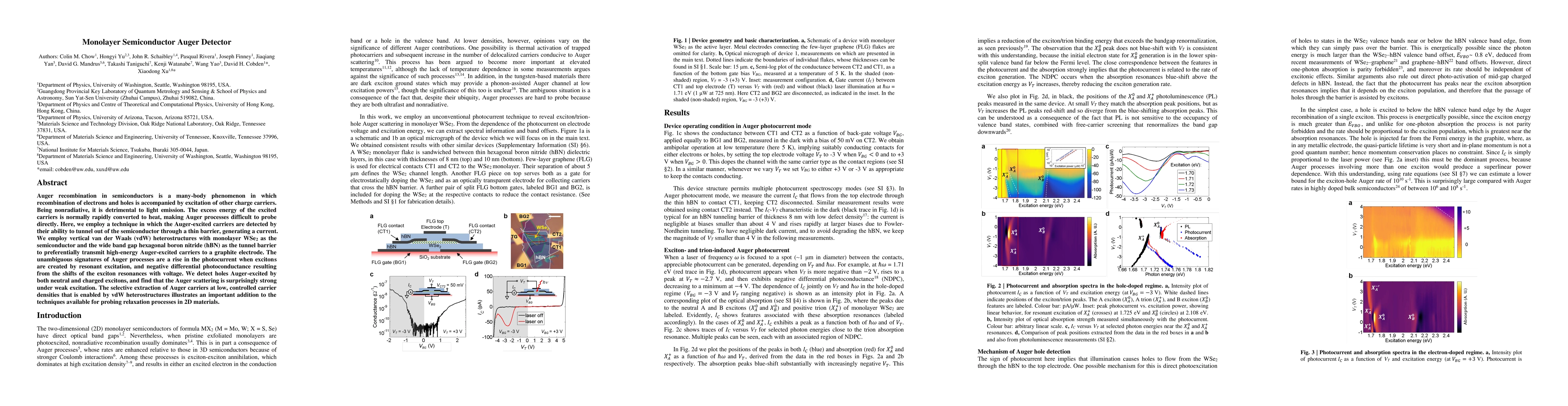
Auger recombination in semiconductors is a many-body phenomenon in which recombination of electrons and holes is accompanied by excitation of other charge carriers. Being nonradiative, it is detrimental to light emission. The excess energy of the excited carriers is normally rapidly converted to heat, making Auger processes difficult to probe directly. Here, we employ a technique in which the Auger-excited carriers are detected by their ability to tunnel out of the semiconductor through a thin barrier, generating a current. We employ vertical van der Waals (vdW) heterostructures with monolayer WSe2 as the semiconductor and the wide band gap hexagonal boron nitride (hBN) as the tunnel barrier to preferentially transmit high-energy Auger-excited carriers to a graphite electrode. The unambiguous signatures of Auger processes are a rise in the photocurrent when excitons are created by resonant excitation, and negative differential photoconductance resulting from the shifts of the exciton resonances with voltage. We detect holes Auger-excited by both neutral and charged excitons, and find that the Auger scattering is surprisingly strong under weak excitation. The selective extraction of Auger carriers at low, controlled carrier densities that is enabled by vdW heterostructures illustrates an important addition to the techniques available for probing relaxation processes in 2D materials.
AI Key Findings
Get AI-generated insights about this paper's methodology, results, significance, and more — seven facets brought into focus.
Impact
Paper Details
Authors
PDF Preview
Key Terms
Citation Network
Current paper (gray), citations (green), references (blue)
Display is limited for performance on very large graphs.
Discussion 0