ArxivLens

Publication

Published: Jul 08, 2026
Categories: cond-mat.mtrl-sci

Metrics

Source: ArXiv

Quick Answers

What methodology did the authors use?

The study employs AlScN gate stacks integrated with GaN transistors, manipulating area-ratio (SMIS/SMFM) to simultaneously access memory and analog functionalities. Fabrication includes devices with low (1,2) and high (4,8) area-ratios, enabling multi-level memory operation and tunable conductance for analog processing, including a GaN ferroelectric frequency-to-voltage converter. Performance characterization centers on memory window, subthreshold swing, conductance state control, inverter multistate operation,... More in Methodology →

What are the key results?

Record memory window of 27 V and forward subthreshold swing of 27 mV/dec achieved by precise control of intermediate electrode length and ferroelectric polarization reversal. — Low area-ratio devices (SMIS/SMFM = 1, 2) demonstrate 4-bit multi-level cell operation with excellent spatial uniformity in a 4x4 array. More in Key Results →

Why is this work significant?

Demonstrates monolithic GaN systems that integrate non-volatile memory with analog processing using area-ratio engineered ferroelectric AlScN gate stacks, offering a pathway for compact, high-power/RF capable neuromorphic and signal-processing hardware with memory-analog co-optimization. More in Significance →

What are the main limitations?

Study focuses on device-scale demonstrations; large-area integration and long-term reliability under high-power/RF operation require further validation. — Lifetime/fatigue performance of ferroelectric AlScN inGaN/GaN stack under repeated polarization switching not exhaustively characterized. More in Limitations →

Paper Preview

Abstract

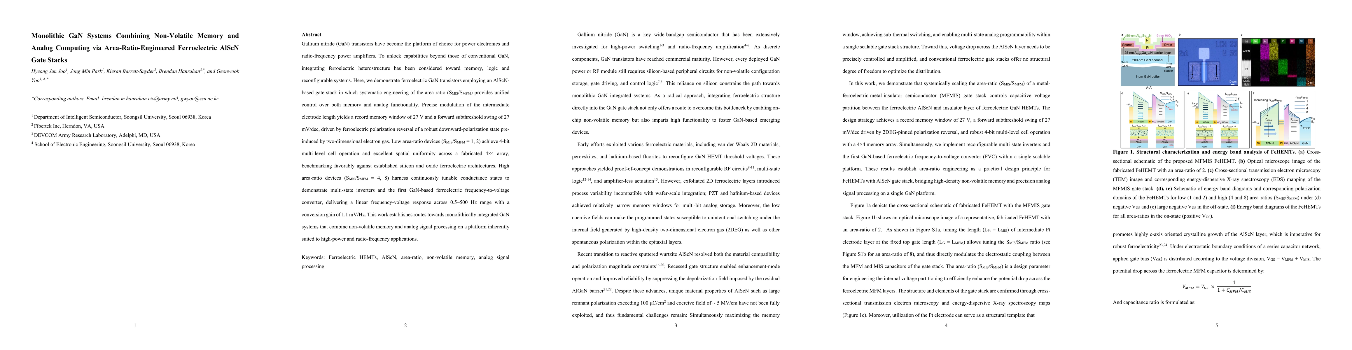
Gallium nitride (GaN) transistors have become the platform of choice for power electronics and radio-frequency power amplifiers. To unlock capabilities beyond those of conventional GaN, integrating ferroelectric heterostructure has been considered toward memory, logic and reconfigurable systems. Here, we demonstrate ferroelectric GaN transistors employing an AlScN-based gate stack in which systematic engineering of the area-ratio (SMIS/SMFM) provides unified control over both memory and analog functionality. Precise modulation of the intermediate electrode length yields a record memory window of 27 V and a forward subthreshold swing of 27 mV/dec, driven by ferroelectric polarization reversal of a robust downward-polarization state pre-induced by two-dimensional electron gas. Low area-ratio devices (SMIS/SMFM = 1, 2) achieve 4-bit multi-level cell operation and excellent spatial uniformity across a fabricated 4 x 4 array, benchmarking favorably against established silicon and oxide ferroelectric architectures. High area-ratio devices (SMIS/SMFM = 4, 8) harness continuously tunable conductance states to demonstrate multi-state inverters and the first GaN-based ferroelectric frequency-to-voltage converter, delivering a linear frequency-voltage response across 0.5 - 500 Hz range with a conversion gain of 1.1 mV/Hz. This work establishes routes towards monolithically integrated GaN systems that combine non-volatile memory and analog signal processing on a platform inherently suited to high-power and radio-frequency applications.
Key Findings, in focus

Seven facets of this paper, analysed and brought into focus by AI.

AI-generated · verify against source Generated Jul 10, 2026
In focus · one-line synthesis

Demonstrates monolithic GaN systems that integrate non-volatile memory with analog processing using area-ratio engineered ferroelectric AlScN gate stacks, offering a pathway for compact, high-power/RF capable neuromorphic and signal-processing hardware with memory-analog co-optimization.

01
MethodologyHow they did it

The study employs AlScN gate stacks integrated with GaN transistors, manipulating area-ratio (SMIS/SMFM) to simultaneously access memory and analog functionalities. Fabrication includes devices with low (1,2) and high (4,8) area-ratios, enabling multi-level memory operation and tunable conductance for analog processing, including a GaN ferroelectric frequency-to-voltage converter. Performance characterization centers on memory window, subthreshold swing, conductance state control, inverter multistate operation, and a linear F-V response across a defined frequency range.

02
ResultsWhat they found
  • Record memory window of 27 V and forward subthreshold swing of 27 mV/dec achieved by precise control of intermediate electrode length and ferroelectric polarization reversal.
  • Low area-ratio devices (SMIS/SMFM = 1, 2) demonstrate 4-bit multi-level cell operation with excellent spatial uniformity in a 4x4 array.
  • High area-ratio devices (SMIS/SMFM = 4, 8) provide continuously tunable conductance states enabling multi-state inverters and the first GaN-based ferroelectric frequency-to-voltage converter with a linear 1.1 mV/Hz gain across 0.5–500 Hz.
03
SignificanceWhy it matters

Demonstrates monolithic GaN systems that integrate non-volatile memory with analog processing using area-ratio engineered ferroelectric AlScN gate stacks, offering a pathway for compact, high-power/RF capable neuromorphic and signal-processing hardware with memory-analog co-optimization.

04
Technical ContributionsWhat's new technically

Introduction of area-ratio engineering (SMIS/SMFM) in AlScN gate-stack GaN transistors to jointly enable non-volatile memory and analog computing, including a record memory window, multi-bit memory in 4x4 arrays, and a GaN ferroelectric frequency-to-voltage converter with linear F-V response.

05
NoveltyWhat sets it apart

First demonstration of monolithic GaN ferroelectric devices that unify memory and analog functions through area-ratio engineered ferroelectric gate stacks, achieving both discrete multi-level storage and continuously tunable conductance with an accompanying frequency-to-voltage conversion capability.

06
LimitationsWhat to be cautious about
  • Study focuses on device-scale demonstrations; large-area integration and long-term reliability under high-power/RF operation require further validation.
  • Lifetime/fatigue performance of ferroelectric AlScN inGaN/GaN stack under repeated polarization switching not exhaustively characterized.
  • Temperature stability and environmental sensitivity of the area-ratio engineered ferroelectric response need broader assessment.
07
Future WorkWhere it goes next
  • Investigate scalability to larger arrays and integration with peripheral circuitry for on-chip signal conditioning.
  • Explore reliability-enhancing integration schemes to mitigate depolarization fields and fatigue in ferroelectric GaN transistors.
  • Extend the architecture to more diversified analog computing primitives and higher-frequency operation targets.

Paper Details

Paper ID: 2607.07577
Comments: 5 figures
Categories:
cond-mat.mtrl-sci

How to Cite This Paper

Reference manager: RIS EndNote


Discussion 0

This website uses cookies to ensure you get the best experience. Learn more