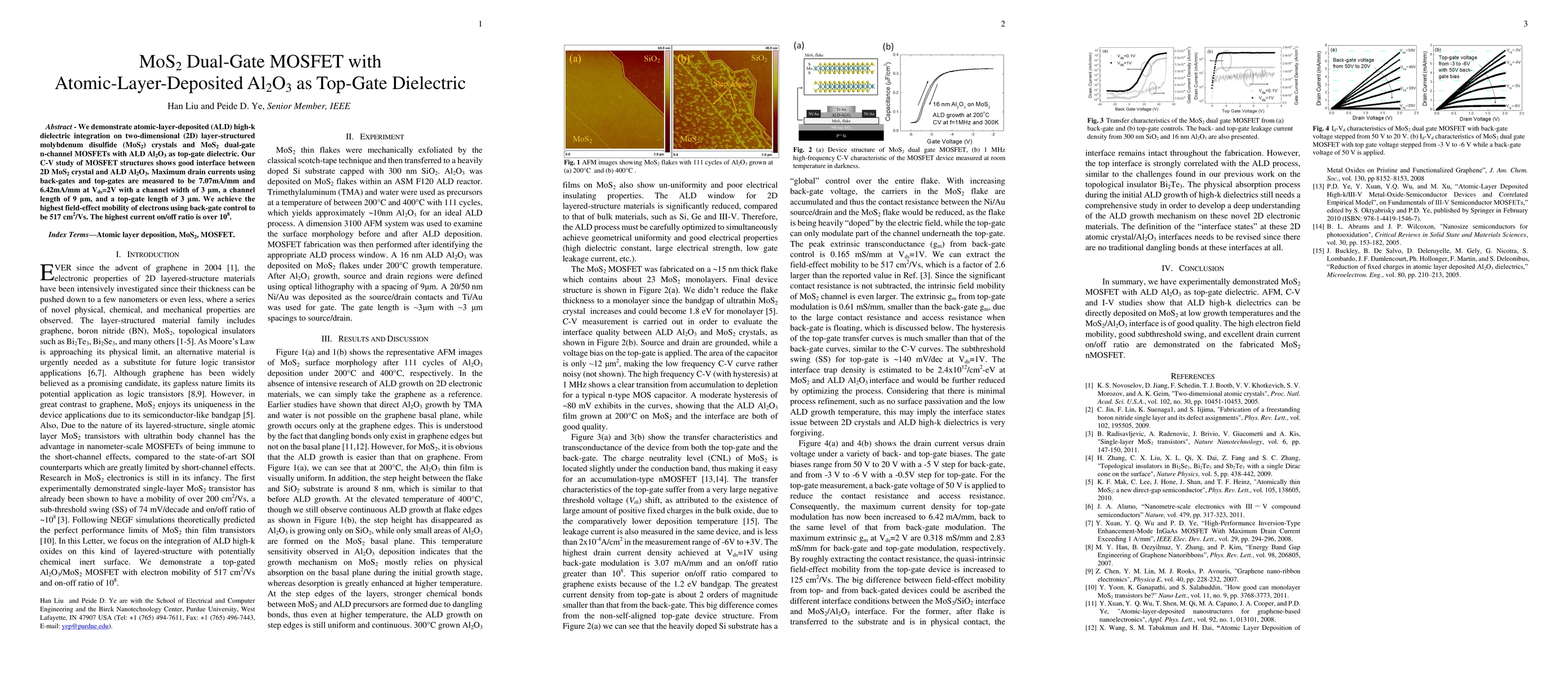
This paper demonstrates the integration of atomic-layer-deposited Al2O3 as a top-gate dielectric in MoS2 dual-gate MOSFETs, achieving high field-effect mobility and a current on/off ratio exceeding 10^8. The study shows excellent interface quality between MoS2 and Al2O3, with maximum drain currents of 7.07mA/mm and 6.42mA/mm for back-gate and top-gate controls, respectively.
We demonstrate atomic-layer-deposited (ALD) high-k dielectric integration on two-dimensional (2D) layer-structured molybdenum disulfide (MoS2) crystals and MoS2 dual-gate n-channel MOSFETs with ALD Al2O3 as top-gate dielectric. Our C-V study of MOSFET structures shows good interface between 2D MoS2 crystal and ALD Al2O3. Maximum drain currents using back-gates and top-gates are measured to be 7.07mA/mm and 6.42mA/mm at Vds=2V with a channel width of 3 {\mu}m, a channel length of 9 {\mu}m, and a top-gate length of 3 {\mu}m. We achieve the highest field-effect mobility of electrons using back-gate control to be 517 cm^2/Vs. The highest current on/off ratio is over 10^8.
This graph shows how this paper is connected to other research. The current paper is shown in dark gray, papers that cite it are in green, and papers it references are in blue. You can:
• Hover over any node to see the paper title
• Click a node to view that paper's details
• Drag nodes to rearrange the graph
• Use the zoom controls (bottom right) to zoom in/out
Title | Authors | Year | Actions |
---|---|---|---|
Adsorption of aluminum precursors on MoS2 toward nucleation of atomic layer deposition
|
Iaan Cho, Jiho Yang, Shimeles Shumi Raya, Bonggeun Shong
|
2025
|
View Paper |
Two-Dimensional Semiconductors for State-of-the-Art Complementary Field-Effect Transistors and Integrated Circuits
|
Meng Liang, Han Yan, Nasrullah Wazir, Changjian Zhou, Zichao Ma
|
2024
|
View Paper |
Enhanced performance of MoS2/SiO2 field-effect transistors by hexamethyldisilazane (HMDS) encapsulation
|
Santu Prasad Jana, Shivangi, Suraina Gupta, A. K. Gupta
|
2024
|
View Paper |
Conformal bilayer h-AlN epitaxy on WS2 by ALD with ultralow leakage current
|
Shin-Yuan Wang, Shu-Jui Chang, Yu-Che Huang, J. Chih, Yu-Chin Lin, Chao-Ching Cheng, I. Radu, Chenming Hu, Chao-Hsin Chien
|
2023
|
View Paper |
Direct atomic layer deposition of ultra-thin Al2O3 and HfO2 films on gold-supported monolayer MoS2
|
E. Schilirò, S. Panasci, A. Mio, G. Nicotra, S. Agnello, B. Pécz, G. Radnóczi, I. Deretzis, A. Magna, F. Roccaforte, R. Nigro, F. Giannazzo
|
2023
|
View Paper |
Tunable Negative Photoconductivity in Encapsulated Ambipolar Tellurene for Functional Optoelectronic Device Applications
|
D. Nguyen, Sangeun Cho, Sunjung Park, D. Park, Hyeong Chan Suh, M. S. Jeong, Thi Phuong Anh Bach, H. Kim, H. Im
|
2023
|
View Paper |
A Van der Waals plug‐and‐probe approach
|
Tiantian Zhou, Deyang Ji
|
2023
|
View Paper |
Recent Developments in Black Phosphorous Transistors: A Review
|
Adhithan Pon, A. Bhattacharyya, Ramesh Rathinam
|
2021
|
View Paper |
Reaction Mechanisms of Non-hydrolytic Atomic Layer Deposition of Al2O3 with a Series of Alcohol Oxidants
|
Seunggi Seo, Whang Je Woo, Yujin Lee, Hwi Yoon, Miso Kim, I. Oh, Seung-Min Chung, Hyungjun Kim, Bonggeun Shong
|
2021
|
View Paper |
Direct Atomic Layer Deposition of Ultrathin Aluminum Oxide on Monolayer MoS2 Exfoliated on Gold: The Role of the Substrate
|
E. Schilirò, R. Nigro, S. Panasci, S. Agnello, M. Cannas, F. Gelardi, F. Roccaforte, F. Giannazzo
|
2021
|
View Paper |
Toward Enhanced Humidity Stability of Triboelectric Mechanical Sensors via Atomic Layer Deposition
|
Wook Kim, Sumaira Yasmeen, C. T. Nguyen, Han‐Bo‐Ram Lee, D. Choi
|
2021
|
View Paper |
High-performance multilayer WSe2 p-type field effect transistors with Pd contacts for circuit applications
|
Lu Zhang, Yadong Zhang, Xiaoting Sun, K. Jia, Qingzhu Zhang, Zhenhua Wu, H. Yin
|
2021
|
View Paper |
Traps at the hBN/WSe2 interface and their impact on polarity transition in WSe2
|
Fida Ali, Faisal Ahmed, Muhammad Taqi, Sekhar Babu Mitta, Tien Dat Ngo, D. Eom, Kenji Watanabe, T. Taniguchi, Hyoungsub Kim, E. Hwang, W. Yoo
|
2021
|
View Paper |
Optical properties of molybdenum disulfide on different substrates affected by spin-orbit coupling
|
Ming-Fang Wei, Yanfeng Zhang, J. Lian, Pengfei Yang, Yujun Shi, Kai Dai, Q. Jiang, Yu Zhang, Chenlin Wang
|
2021
|
View Paper |
WITHDRAWN: Design and analysis of broadband Terahertz absorber based on multi-layer and multi-ribbon structures of molybdenum disulfide
|
Erfan Dejband, Pouya Torkaman, M. J. Mohammad-Zamani
|
2021
|
View Paper |
Dual-gate MoS2 phototransistor with atomic-layer-deposited HfO2 as top-gate dielectric for ultrahigh photoresponsivity
|
Xiaoxi Li, Xinyu Chen, Jin-Xin Chen, Guang Zeng, Yu-Chun Li, Wei Huang, Zhigang Ji, David-Wei Zhang, H. Lu
|
2021
|
View Paper |
Benchmarking monolayer MoS2 and WS2 field-effect transistors
|
Amritanand Sebastian, Rahul Pendurthi, T. Choudhury, J. Redwing, Saptarshi Das
|
2021
|
View Paper |
How good are 2D transistors? An application-specific benchmarking study
|
Hattan Abuzaid, Nicholas X. Williams, A. Franklin
|
2021
|
View Paper |
Hf₀.₅Zr₀.₅O₂ Ferroelectric Embedded Dual-Gate MoS₂ Field Effect Transistors for Memory Merged Logic Applications
|
Kailiang Huang, Minglong Zhai, Xueyuan Liu, Bing Sun, Hudong Chang, Jianhua Liu, Chao Feng, Honggang Liu
|
2020
|
View Paper |
ALD-ZrO2 gate dielectric with suppressed interfacial oxidation for high performance MoS2 top gate MOSFETs
|
W. Chang, N. Okada, M. Horikawa, T. Endo, Y. Miyata, T. Irisawa
|
2020
|
View Paper |
2D-MoS2/BMN Ceramic Hybrid Structure Flexible TFTs with Tunable Device Properties.
|
Junqing Wei, Shihui Yu, X. Shan, Kuibo Lan, Xiaodong Yang, Kailiang Zhang, G. Qin
|
2020
|
View Paper |
Titanium disulfide as Schottky/ohmic contact for monolayer molybdenum disulfide
|
Junsen Gao, Manisha Gupta
|
2020
|
View Paper |
Insulators for 2D nanoelectronics: the gap to bridge
|
Y. Illarionov, T. Knobloch, M. Jech, M. Lanza, D. Akinwande, M. Vexler, T. Mueller, M. Lemme, G. Fiori, F. Schwierz, T. Grasser
|
2020
|
View Paper |
Large-area 2D TMD layers for mechanically reconfigurable electronic devices
|
T. Ko, Mengjing Wang, Changhyeon Yoo, E. Okogbue, Md. Ashraful Islam, Hao Li, M. S. Shawkat, S. Han, K. Oh, Yeonwoong Jung
|
2020
|
View Paper |
Direct CVD Growth of a Graphene/MoS2 Heterostructure with Interfacial Bonding for Two-Dimensional Electronics
|
Eunho Lee, Seung Goo Lee, Wi Hyoung Lee, H. Lee, N. Nguyen, Min Seok Yoo, Kilwon Cho
|
2020
|
View Paper |
Vapor phase processing: a novel approach for fabricating functional hybrid materials
|
Karina Ashurbekova, Kristina Ashurbekova, Gabriele A Botta, O. Yurkevich, Mato Knez
|
2020
|
View Paper |
Low-Temperature Physical Adsorption for the Nucleation of Sub-10 nm Al2O3 Gate Stack on Top-Gated WS2 Transistors
|
Yu-Shu Lin, Juyea Hoo, Tsai-Fu Chung, J. Yang, Miin-Jang Chen
|
2020
|
View Paper |
Electrical Properties of MoS2 Field-Effect Transistors in Contact with Layered CrPS4
|
Min-Seon Shin, Mi Jung Lee, Ji Hye Lee, B. Park, Sungmin Lee, Je-Guen Park
|
2020
|
View Paper |
High-Performance Logic and Memory Devices Based on a Dual-Gated MoS2 Architecture
|
Fuyou Liao, Zhongxun Guo, Yin Wang, Yufeng Xie, Simeng Zhang, Y. Sheng, Hongwei Tang, Zihan Xu, A. Riaud, P. Zhou, J. Wan, M. Fuhrer, Xiangwei Jiang, D. Zhang, Y. Chai, W. Bao
|
2019
|
View Paper |
Uniform and ultrathin high-κ gate dielectrics for two-dimensional electronic devices
|
Weisheng Li, Jian Zhou, S. Cai, Zhihao Yu, Jialin Zhang, N. Fang, Taotao Li, Yun Wu, Tangsheng Chen, Xiaoyu Xie, Hai-bo Ma, Ke Yan, N. Dai, Xiangjin Wu, Huijuan Zhao, Zixuan Wang, Daowei He, Lijia Pan, Yi Shi, Peng Wang, Wei Chen, K. Nagashio, X. Duan, Xinran Wang
|
2019
|
View Paper |
Efficient passivation of monolayer MoS2 by epitaxially grown 2D organic crystals.
|
Xin Xu, Zefeng Chen, Beilei Sun, Yu Zhao, Li Tao, Jian-bin Xu
|
2019
|
View Paper |
The evolution of MoS2 properties under oxygen plasma treatment and its application in MoS2 based devices
|
Yadong Zhang, Jiangtao Liu, Yu Pan, Kun Luo, Jiahan Yu, Yongkui Zhang, K. Jia, H. Yin, Huilong Zhu, Hanmin Tian, Zhenhua Wu
|
2019
|
View Paper |
Quantum-mechanical effect in atomically thin MoS2 FET
|
N. Fang, K. Nagashio
|
2019
|
View Paper |
MoS2 dual-gate transistors with electrostatically doped contacts
|
Fuyou Liao, Y. Sheng, Zhongxun Guo, Hongwei Tang, Yin Wang, Lingyi Zong, Xinyu Chen, A. Riaud, Jiahe Zhu, Yufeng Xie, Lin Chen, Hao Zhu, Qingqing Sun, P. Zhou, Xiangwei Jiang, J. Wan, W. Bao, David-Wei Zhang
|
2019
|
View Paper |
Photoresponse of homostructure WSe2 rectifying diode
|
T. Peng, Chung-Hung Hong, Ming-Ru Tang, Si-Chen Lee
|
2019
|
View Paper |
Reduced interfacial fluctuation leading enhanced mobility in a monolayer MoS2 DG FET under low vertical electric field
|
H. Ji, Hojoon Yi, Sakong Wonkil, H. Kim, S. Lim
|
2019
|
View Paper |
Prediction of two-dimensional monochalcogenides: MoS and WS
|
Dhanshree Pandey, A. Chakrabarti
|
2019
|
View Paper |
Ultrathin monolithic HfO2 formed by Hf-seeded atomic layer deposition on MoS2: Film characteristics and its transistor application
|
Hoijoon Kim, Taejin Park, Seongjae Park, Mirine Leem, W. Ahn, Hyangsook Lee, Changmin Lee, Eunha Lee, Seong-Jun Jeong, Seongjun Park, Yunseok Kim, Hyoungsub Kim
|
2019
|
View Paper |
Microscopic observation of catalytically etched channels and pits in MoS2 flakes
|
Do-Hyun Kim, J. Choi, J. Jin, D. J. Lee, Gyu-Tae Kim
|
2019
|
View Paper |
Trapped charge modulation at the MoS2/SiO2 interface by a lateral electric field in MoS2 field-effect transistors
|
Jinsu Pak, Kyungjun Cho, Jae‐Keun Kim, Y. Jang, Jiwon Shin, Jaeyoung Kim, Junseok Seo, Seungjun Chung, Takhee Lee
|
2019
|
View Paper |
Short-channel effects on the static noise margin of 6T SRAM composed of 2D semiconductor MOSFETs
|
Qian Xie, Chen Chen, Mingjun Liu, Shuang Xia, Z. Wang
|
2019
|
View Paper |
Low-voltage electric-double-layer MoS2 transistor gated via water solution
|
Junjie Guo, Jie Jiang, Bingchu Yang
|
2018
|
View Paper |
Significant enhancement of photoresponsive characteristics and mobility of MoS2-based transistors through hybridization with perovskite CsPbBr3 quantum dots
|
T. Noh, Heung Seob Shin, Changwon Seo, Jun Young Kim, Jongwon Youn, Jeongyong Kim, K. Lee, J. Joo
|
2018
|
View Paper |
UV-Ozone Functionalization of 2D Materials
|
S. McDonnell, R. Wallace
|
2018
|
View Paper |
Research progress and challenges of two dimensional MoS2 field effect transistors
|
N. Divya Bharathi, K. Sivasankaran
|
2018
|
View Paper |
Charge carrier injection and transport engineering in two-dimensional transition metal dichalcogenides
|
J. D. Durán Retamal, Dharmaraj Periyanagounder, Jr-jian Ke, M. Tsai, Jr-hau He
|
2018
|
View Paper |
High-Vacuum Particulate-Free Deposition of Wafer-Scale Mono-, Bi-, and Trilayer Molybdenum Disulfide with Superior Transport Properties.
|
Kortney Almeida, Michelle Wurch, A. Geremew, K. Yamaguchi, Thomas A. Empante, Michael D. Valentin, Michael G. Gomez, Adam J. Berges, G. Stecklein, S. Rumyantsev, Joseph Martinez, A. Balandin, L. Bartels
|
2018
|
View Paper |
High carrier mobility in monolayer CVD-grown MoS2 through phonon suppression.
|
Nengjie Huo, Yujue Yang, Yu-Ning Wu, Xiaoguang Zhang, S. Pantelides, G. Konstantatos
|
2018
|
View Paper |
Recent Progress and Future Prospects of 2D‐Based Photodetectors
|
Nengjie Huo, G. Konstantatos
|
2018
|
View Paper |
Enhanced sulfurization reaction of molybdenum using a thermal cracker for forming two-dimensional MoS2 layers.
|
Dae‐Hyung Cho, Woo-Jung Lee, Jae-Hyung Wi, W. Han, S. Yun, B. Shin, Yong‐Duck Chung
|
2018
|
View Paper |
Atomic layer deposition of sub-10 nm high-K gate dielectrics on top-gated MoS2 transistors without surface functionalization
|
Yu-Shu Lin, Po-Hsien Cheng, K. Huang, Hsin-Chih Lin, Miin-Jang Chen
|
2018
|
View Paper |
Low-power logic computing realized in a single electric-double-layer MoS 2 transistor gated with polymer electrolyte
|
Junjie Guo, Dingdong Xie, Bingchu Yang, Jie Jiang
|
2018
|
View Paper |
Very fast hot carrier diffusion in unconstrained MoS2 on a glass substrate: discovered by picosecond ET-Raman
|
Pengyu Yuan, H. Tan, Ridong Wang, Tianyu Wang, Xinwei Wang
|
2018
|
View Paper |
Near-zero hysteresis and near-ideal subthreshold swing in h-BN encapsulated single-layer MoS2 field-effect transistors
|
Q. Vu, Sidi Fan, Sang Hyup Lee, Min-Kyu Joo, W. Yu, Young Hee Lee
|
2018
|
View Paper |
Growth of atomically thin MoS2 flakes on high-κ substrates by chemical vapor deposition
|
Mei Zhao, Lijie Zhang, Manman Liu, Youqing Dong, Chao Zou, Yue Hu, Keqin Yang, Yun Yang, H. Zeng, Shaoming Huang
|
2018
|
View Paper |
Band alignment of In2Se3 multilayers/ZnO heterojunction measured by X-ray photoelectron spectroscopy
|
H. Zhang, S. Yan, S. Li, S. Su
|
2018
|
View Paper |
Temperature-dependent properties of monolayer MoS2 annealed in an Ar diluted S atmosphere: an experimental and first-principles study
|
Lei Wang, X. Ji, Fei Chen, Qinyuan Zhang
|
2017
|
View Paper |
Carrier‐Type Modulation and Mobility Improvement of Thin MoTe2
|
Deshun Qu, Xiaochi Liu, Ming Huang, Changmin Lee, Faisal Ahmed, Hyoungsub Kim, R. Ruoff, J. Hone, W. Yoo
|
2017
|
View Paper |
Vertical Charge Transport and Negative Transconductance in Multilayer Molybdenum Disulfides.
|
Yuan Liu, Jian Guo, Qiyuan He, Hao Wu, Hung-Chieh Cheng, Mengning Ding, I. Shakir, V. Gambin, Yu Huang, X. Duan
|
2017
|
View Paper |
Two-Dimensional Transition Metal Dichalcogenides and Their Charge Carrier Mobilities in Field-Effect Transistors
|
Sohail Ahmed, J. Yi
|
2017
|
View Paper |
Effect of Carrier Localization on Electrical Transport and Noise at Individual Grain Boundaries in Monolayer MoS2.
|
Kimberly Hsieh, V. Kochat, Xiang Zhang, Y. Gong, C. Tiwary, P. Ajayan, A. Ghosh
|
2017
|
View Paper |
HfSe2 and ZrSe2: Two-dimensional semiconductors with native high-κ oxides
|
M. Mleczko, Chaofan Zhang, H. Lee, H. Kuo, B. Magyari-Köpe, R. Moore, Z. Shen, I. Fisher, Y. Nishi, E. Pop
|
2017
|
View Paper |
Transistors and tunnel diodes enabled by large-scale MoS2 nanosheets grown on GaN
|
P. Yip, Xinbo Zou, W. C. Cho, K. L. Wu, K. Lau
|
2017
|
View Paper |
Demonstration of 2e12cm2eV1 2D-oxide interface trap density on back-gated MoS2 flake devices with 2.5nm EOT
|
A. Gaur, Y. Balaji, D. Lin, C. Adelmann, J. V. Houdt, M. Heyns, D. Mocuta, I. Radu
|
2017
|
View Paper |
Electrically induced, non-volatile, metal insulator transition in a ferroelectric-controlled MoS2 transistor
|
Zhongyuan Lu, C. Serrao, A. Khan, J. Clarkson, Justin C. Wong, R. Ramesh, S. Salahuddin
|
2017
|
View Paper |
Resistive switching in MoSe$_{2}$/BaTiO$_{3}$ hybrid structures
|
J. P. B. Silva, C. A. Marques, J. A. Moreira, O. Conde
|
2017
|
View Paper |
Performance Limits of the Self‐Aligned Nanowire Top‐Gated MoS2 Transistors
|
Zhenyu Yang, Xingqiang Liu, Xuming Zou, Jingli Wang, Chao Ma, Changzhong Jiang, J. Ho, Caofeng Pan, Xiangheng Xiao, J. Xiong, L. Liao
|
2017
|
View Paper |
Effects of high-k dielectric environment on the full ballistic transport properties of monolayer MoS2 FETs
|
Xian-Jiang Song, Lichun Xu, Hui Bai, Ying Li, Zhiyuan Ma, Zhi Yang, Ruiping Liu, Xiuyan Li
|
2017
|
View Paper |
Split-gated point-contact for electrostatic confinement of transport in MoS2/h-BN hybrid structures
|
C. Sharma, M. Thalakulam
|
2017
|
View Paper |
Electronic and Optoelectronic Devices based on Two‐Dimensional Materials: From Fabrication to Application
|
Jaewoo Shim, Hyung‐Youl Park, D. Kang, Jinok Kim, Seo-Hyeon Jo, Yongkook Park, Jin-Hong Park
|
2017
|
View Paper |
Investigation of chemical vapour deposition MoS2 field effect transistors on SiO2 and ZrO2 substrates
|
X. Liu, Y. Chai, Zhaojun Liu
|
2017
|
View Paper |
Forming free and ultralow-power erase operation in atomically crystal TiO2 resistive switching
|
Ya-Wei Dai, W. Bao, Linfeng Hu, Chunsen Liu, Xiaowen Yan, Lin Chen, Qingqing Sun, S. Ding, P. Zhou, David-Wei Zhang
|
2017
|
View Paper |
Impact and Origin of Interface States in MOS Capacitor with Monolayer MoS2 and HfO2 High-k Dielectric
|
P. Xia, Xuewei Feng, Rui Jie Ng, Shijie Wang, D. Chi, Cequn Li, Zhubing He, Xinke Liu, K. Ang
|
2017
|
View Paper |
Atomic layer deposition of Al2O3 on MoS2, WS2, WSe2, and h-BN: surface coverage and adsorption energy
|
Taejin Park, Hoijoon Kim, Mirine Leem, W. Ahn, Seongheum Choi, Jinbum Kim, Joon Uh, Kee-Won Kwon, Seong-Jun Jeong, Seongjun Park, Yunseok Kim, Hyoungsub Kim
|
2017
|
View Paper |
Solution‐processed high‐k oxide dielectric via deep ultraviolet and rapid thermal annealing for high‐performance MoS2 FETs
|
G. Yoo, Sol Lea Choi, B. Yoo, M. Oh
|
2017
|
View Paper |
Nitride Dielectric Environments to Suppress Surface Optical Phonon Dominated Scattering in High‐Performance Multilayer MoS2 FETs
|
Shubhadeep Bhattacharjee, K. L. Ganapathi, Hareesh Chandrasekar, Tathagata Paul, S. Mohan, A. Ghosh, S. Raghavan, N. Bhat
|
2017
|
View Paper |
Investigations of vapour-phase deposited transition metal dichalcogenide films for future electronic applications
|
Riley Gatensby, T. Hallam, Kangho Lee, N. McEvoy, G. Duesberg
|
2016
|
View Paper |
The transport properties of the Phosphorus and Chlorine doped single layer MoS 2 p-n junctions: A first-principles study
|
Qingyi Zeng, Jiangling Pan, Zhixiong Yang, Shenglin Peng, H. Zou, Fangping Ouyang
|
2016
|
View Paper |
Two-dimensional inorganic analogues of graphene: transition metal dichalcogenides
|
Manoj K. Jana, C. Rao
|
2016
|
View Paper |
Performance Upper Limit of sub‐10 nm Monolayer MoS2 Transistors
|
Yiwei Zhao, Yan Li, Fei Ma
|
2016
|
View Paper |
First-principles investigation on the interface of transition metal dichalcogenide MX2 (M = Mo, W; X = S, Se) monolayer on Al2O3(0 0 0 1)
|
Rui Pan, Xiaoli Fan, Han Zhang, Yi Yang
|
2016
|
View Paper |
Photodetectors based on two dimensional materials
|
Zheng 正 Lou 娄, Zhongzhu 中翥 Liang 梁, Guozhen 国震 Shen 沈
|
2016
|
View Paper |
2D layered group IIIA metal chalcogenides: synthesis, properties and applications in electronics and optoelectronics
|
Wenjuan Huang, Lin Gan, Huiqiao Li, Ying Ma, T. Zhai
|
2016
|
View Paper |
Low energy ion scattering (LEIS). A practical introduction to its theory, instrumentation, and applications
|
Cody V. Cushman, P. Brüner, J. Zakel, George H. Major, B. Lunt, N. Smith, T. Grehl, M. Linford
|
2016
|
View Paper |
Absorption enhancement in CH3NH3PbI3 solar cell using a TiO2/MoS2 nanocomposite electron selective contact
|
Muhammad Imran Ahmed, Z. Hussain, Amir Khalid, Hafiz M. F. Amin, A. Habib
|
2016
|
View Paper |
Atomically Thin MoS2: A Versatile Nongraphene 2D Material
|
Y. Subbaiah, K. Saji, A. Tiwari
|
2016
|
View Paper |
Thickness-dependent charge transport in few-layer MoS2 field-effect transistors
|
Ming-Wei Lin, I. Kravchenko, J. Fowlkes, Xufan Li, A. Puretzky, C. Rouleau, D. Geohegan, Kai Xiao
|
2016
|
View Paper |
Controlled Sulfurization Process for the Synthesis of Large Area MoS2 Films and MoS2/WS2 Heterostructures
|
D. Chiappe, I. Asselberghs, S. Sutar, S. Iacovo, V. Afanas’ev, A. Stesmans, Y. Balaji, Lisanne Peters, M. Heyne, M. Mannarino, W. Vandervorst, S. Sayan, C. Huyghebaert, M. Caymax, M. Heyns, S. De Gendt, I. Radu, A. Thean
|
2016
|
View Paper |
Band alignment of atomic layer deposited high-k Al2O3/multilayer MoS2 interface determined by X-ray photoelectron spectroscopy
|
Xinke Liu, Le Chen, Qiang Liu, Jiazhu He, Kuilong Li, Wenjie Yu, J. Ao, K. Ang
|
2015
|
View Paper |
Controlled Doping of Vacancy-Containing Few-Layer MoS2 via Highly Stable Thiol-Based Molecular Chemisorption.
|
D. Sim, Mincheol Kim, S. Yim, Min‐Jae Choi, Jaesuk Choi, S. Yoo, Y. Jung
|
2015
|
View Paper |
Electrical characterization of top-gated molybdenum disulfide metal-oxide-semiconductor capacitors with high-k dielectrics
|
P. Zhao, P. Vyas, S. McDonnell, Pavel Bolshakov-Barrett, A. Azcatl, C. Hinkle, P. Hurley, R. Wallace, C. Young
|
2015
|
View Paper |
Ab-initio study of dynamical properties of two dimensional MoS2 under strain
|
H. Soni, P. Jha
|
2015
|
View Paper |
Functional Nanomaterial Devices
|
J. Pu, T. Takenobu
|
2015
|
View Paper |
Recent development in 2D materials beyond graphene
|
Ankur Gupta, T. Sakthivel, S. Seal
|
2015
|
View Paper |
Ionic Liquid Gating of Suspended MoS2 Field Effect Transistor Devices.
|
Fenglin Wang, P. Stepanov, Mason J Gray, C. N. Lau, M. Itkis, R. Haddon
|
2015
|
View Paper |
Metal Semiconductor Field-Effect Transistor with MoS2/Conducting NiO(x) van der Waals Schottky Interface for Intrinsic High Mobility and Photoswitching Speed.
|
H. Lee, S. Baik, Kimoon Lee, S. Min, P. Jeon, Jin Sung Kim, Kyujin Choi, H. Choi, Jae Hoon Kim, S. Im
|
2015
|
View Paper |
The Integration of Sub-10 nm Gate Oxide on MoS2 with Ultra Low Leakage and Enhanced Mobility
|
Wen Yang, Qingqing Sun, Y. Geng, Lin Chen, P. Zhou, S. Ding, David-Wei Zhang
|
2015
|
View Paper |
Electronic, dielectric and mechanical properties of MoS2/SiC hybrid bilayer: A first principle study
|
Munish Sharma, Pooja Jamdagni, Ashok Kumar, P. Ahluwalia
|
2015
|
View Paper |
Air Stable Doping and Intrinsic Mobility Enhancement in Monolayer Molybdenum Disulfide by Amorphous Titanium Suboxide Encapsulation.
|
A. Rai, Amithraj Valsaraj, Hema C. P. Movva, A. Roy, R. Ghosh, S. Sonde, Sangwoo Kang, Jiwon Chang, Tanuj Trivedi, Rik Dey, S. Guchhait, S. Larentis, L. F. Register, E. Tutuc, S. Banerjee
|
2015
|
View Paper |
Thin‐Film Transistors Based on Transition Metal Dichalcogenides
|
Woong Choi, Sunkook Kim
|
2015
|
View Paper |
Comparative Study on Electronic Structures of Sc and Ti Contacts with Monolayer and Multilayer MoS2.
|
Zhongjun Li, Xingxing Li, Jinlong Yang
|
2015
|
View Paper |
Chemical doping of MoS2 multilayer by p-toluene sulfonic acid
|
S. Andleeb, Arun Kumar Singh, J. Eom
|
2015
|
View Paper |
Photocurrent generation with two-dimensional van der Waals semiconductors.
|
M. Buscema, J. Island, D. Groenendijk, Sofya I. Blanter, G. Steele, H. S. van der Zant, A. Castellanos-Gomez
|
2015
|
View Paper |
Low voltage and high ON/OFF ratio field-effect transistors based on CVD MoS2 and ultra high-k gate dielectric PZT.
|
Changjian Zhou, Xinsheng Wang, S. Raju, Ziyuan Lin, D. Villaroman, Baoling Huang, H. L. Chan, M. Chan, Y. Chai
|
2015
|
View Paper |
Physical and chemical tuning of two-dimensional transition metal dichalcogenides.
|
Haotian Wang, Hongtao Yuan, Seung Sae Hong, Yanbin Li, Yi Cui
|
2015
|
View Paper |
High-quality, large-area MoSe2 and MoSe2/Bi2Se3 heterostructures on AlN(0001)/Si(111) substrates by molecular beam epitaxy.
|
E. Xenogiannopoulou, P. Tsipas, K. Aretouli, D. Tsoutsou, S. A. Giamini, C. Bazioti, G. Dimitrakopulos, P. Komninou, S. Brems, Cedric Huyghebaert, Iuliana Radu, Athanasios Dimoulas
|
2015
|
View Paper |
First-principle study on the optical response of phosphorene
|
Jiahe Lin, Hong Zhang, Xinlu Cheng
|
2015
|
View Paper |
Giant Photoamplification in Indirect‐Bandgap Multilayer MoS2 Phototransistors with Local Bottom‐Gate Structures
|
Junyeon Kwon, Y. Hong, Gyuchull Han, I. Omkaram, Woong Choi, Sunkook Kim, Y. Yoon
|
2015
|
View Paper |
Trap density probing on top-gate MoS₂ nanosheet field-effect transistors by photo-excited charge collection spectroscopy.
|
Kyunghee Choi, S. Raza, H. Lee, P. Jeon, Atiye Pezeshki, S. Min, Jin Sung Kim, Woojin Yoon, Sang-Yong Ju, Kimoon Lee, S. Im
|
2015
|
View Paper |
Science and technology roadmap for graphene, related two-dimensional crystals, and hybrid systems.
|
A. Ferrari, F. Bonaccorso, V. Fal’ko, K. Novoselov, S. Roche, P. Bøggild, S. Borini, F. Koppens, V. Palermo, Nicola Maria Pugno, J. Garrido, R. Sordan, A. Bianco, L. Ballerini, M. Prato, E. Lidorikis, J. Kivioja, C. Marinelli, T. Ryhänen, A. Morpurgo, J. Coleman, V. Nicolosi, L. Colombo, A. Fert, M. García-Hernández, A. Bachtold, G. Schneider, F. Guinea, C. Dekker, M. Barbone, Zhipei Sun, C. Galiotis, A. Grigorenko, G. Konstantatos, A. Kis, M. Katsnelson, L. Vandersypen, Annick Loiseau, V. Morandi, D. Neumaier, E. Treossi, V. Pellegrini, M. Polini, A. Tredicucci, Gareth M Williams, B. Hong, Jong-Hyun Ahn, Jong M. Kim, H. Zirath, B. V. van Wees, H. V. D. van der Zant, L. Occhipinti, Andrea Di Matteo, I. Kinloch, T. Seyller, E. Quesnel, Xinliang Feng, K. Teo, N. Rupesinghe, P. Hakonen, Simon R. T. Neil, Quentin Tannock, T. Löfwander, J. Kinaret
|
2015
|
View Paper |
Layer number dependence of MoS2 photoconductivity using photocurrent spectral atomic force microscopic imaging.
|
Y. Son, Qing Hua Wang, J. Paulson, C. Shih, A. Rajan, K. Tvrdy, Sojin Kim, B. Alfeeli, R. Braatz, M. Strano
|
2015
|
View Paper |
First principle defect study of MoSe2 field effect transistor
|
Bahniman Ghosh, N. Kishor
|
2015
|
View Paper |
An ab initio study of strained two-dimensional MoSe2
|
Bahniman Ghosh, N. Kishor
|
2015
|
View Paper |
Layer-controlled CVD growth of large-area two-dimensional MoS2 films.
|
Jaeho Jeon, S. Jang, S. Jeon, Gwangwe Yoo, Y. H. Jang, Jin-Hong Park, Sungjoo Lee
|
2015
|
View Paper |
Theoretical and experimental investigation of vacancy-based doping of monolayer MoS2 on oxide
|
Amithraj Valsaraj, Jiwon Chang, A. Rai, L. F. Register, S. Banerjee
|
2014
|
View Paper |
Toward barrier free contact to molybdenum disulfide using graphene electrodes.
|
Yuan Liu, Hao Wu, Hung-Chieh Cheng, Sen Yang, Enbo Zhu, Qiyuan He, Mengning Ding, Dehui Li, Jian Guo, Nathan O. Weiss, Yu Huang, X. Duan
|
2014
|
View Paper |
Air-stable transport in graphene-contacted, fully encapsulated ultrathin black phosphorus-based field-effect transistors.
|
A. Avsar, I. J. Vera-Marun, J. Tan, Kenji Watanabe, T. Taniguchi, A. H. Castro Neto, B. Özyilmaz
|
2014
|
View Paper |
Contact-dependent susceptibility and immunity to short-channel effects in monolayer MoS2 field-effect transistors
|
Gyuchull Han, Y. Yoon
|
2014
|
View Paper |
Phase-engineered low-resistance contacts for ultrathin MoS2 transistors.
|
R. Kappera, D. Voiry, S. Yalcin, B. Branch, Gautam Gupta, A. Mohite, M. Chhowalla
|
2014
|
View Paper |
Semiconducting black phosphorus: synthesis, transport properties and electronic applications.
|
Han Liu, Yuchen Du, Yexin Deng, P. Ye
|
2014
|
View Paper |
Stable charge storing in two-dimensional MoS2 nanoflake floating gates for multilevel organic flash memory.
|
Minji Kang, Yeong-a Kim, Jin‐Mun Yun, Dongyoon Khim, Jihong Kim, Yong‐Young Noh, Kang‐Jun Baeg, Dong‐Yu Kim
|
2014
|
View Paper |
Electrical breakdown of multilayer MoS2 field-effect transistors with thickness-dependent mobility.
|
R. Yang, Zenghui Wang, P. Feng
|
2014
|
View Paper |
Few-layer molybdenum disulfide transistors and circuits for high-speed flexible electronics
|
Rui Cheng, Shanjuan Jiang, Yu Chen, Yuan Liu, Nathan O. Weiss, Hung-Chieh Cheng, Hao Wu, Yu Huang, X. Duan
|
2014
|
View Paper |
Study of Electron Transport in Organic and Inorganic Atomic Monolayer Based MOS/MOSFET
|
J. Azariah, U. Satheesh, D.Devaprakasam
|
2014
|
View Paper |
Interface Engineering for High‐Performance Top‐Gated MoS2 Field‐Effect Transistors
|
Xuming Zou, Jingli Wang, Chung‐Hua Chiu, Yun Wu, Xiangheng Xiao, Changzhong Jiang, Wen‐Wei Wu, Liqiang Mai, Tangsheng Chen, Jinchai Li, J. C. Ho, L. Liao
|
2014
|
View Paper |
Two-dimensional TaSe2 metallic crystals: spin-orbit scattering length and breakdown current density.
|
A. Neal, Yuchen Du, Han Liu, P. Ye
|
2014
|
View Paper |
Charge transport in ion-gated mono-, bi-, and trilayer MoS2 field effect transistors
|
L. Chu, H. Schmidt, J. Pu, Shunfeng Wang, B. Özyilmaz, T. Takenobu, G. Eda
|
2014
|
View Paper |
Flexible and stretchable thin-film transistors based on molybdenum disulphide.
|
J. Pu, Lain‐Jong Li, T. Takenobu
|
2014
|
View Paper |
High performance photocatalytic metal oxide synthetic bi-component nanosheets formed by atomic layer deposition
|
Kyoungmi Lee, M. Losego, Do Han Kim, G. Parsons
|
2014
|
View Paper |
Tuning on-off current ratio and field-effect mobility in a MoS(2)-graphene heterostructure via Schottky barrier modulation.
|
C. Shih, Qing Hua Wang, Y. Son, Zhong Jin, D. Blankschtein, M. Strano
|
2014
|
View Paper |
Field-effect transistors built from all two-dimensional material components.
|
T. Roy, M. Tosun, Jeong Seuk Kang, A. Sachid, S. Desai, M. Hettick, C. Hu, A. Javey
|
2014
|
View Paper |
Few-layer MoS2: a promising layered semiconductor.
|
R. Ganatra, Qing Zhang
|
2014
|
View Paper |
Electroluminescence and Photocurrent Generation from Atomically Sharp WSe2/MoS2 Heterojunction p–n Diodes
|
Rui Cheng, Dehui Li, Hailong Zhou, Chen Wang, Anxiang Yin, Shanjuan Jiang, Yuan Liu, Yu Chen, Yu Huang, X. Duan
|
2014
|
View Paper |
Graphene/MoS2 hybrid technology for large-scale two-dimensional electronics.
|
Lili Yu, Yi‐Hsien Lee, X. Ling, E. Santos, Y. C. Shin, Yuxuan Lin, M. Dubey, E. Kaxiras, J. Kong, Han Wang, T. Palacios
|
2014
|
View Paper |
Fabrication and electrical properties of MoS2 nanodisc-based back-gated field effect transistors
|
Weixia Gu, J. Shen, Xiying Ma
|
2014
|
View Paper |
Emerging device applications for semiconducting two-dimensional transition metal dichalcogenides.
|
Deep Jariwala, V. Sangwan, L. Lauhon, T. Marks, M. Hersam
|
2014
|
View Paper |
Phosphorene: an unexplored 2D semiconductor with a high hole mobility.
|
Han Liu, A. Neal, Zhen Zhu, Zhe Luo, Xianfan Xu, D. Tománek, P. Ye
|
2014
|
View Paper |
Low-frequency noise in multilayer MoS2 field-effect transistors: the effect of high-k passivation.
|
Junhong Na, Min-Kyu Joo, M. Shin, J. Huh, Jae-Sung Kim, Mingxing Piao, J. Jin, Ho-Kyun Jang, H. J. Choi, Joon Hyung Shim, Gyu-Tae Kim
|
2014
|
View Paper |
Switching mechanism in single-layer molybdenum disulfide transistors: an insight into current flow across Schottky barriers.
|
Han Liu, M. Si, Yexin Deng, A. Neal, Yuchen Du, S. Najmaei, P. Ajayan, J. Lou, P. Ye
|
2013
|
View Paper |
Direct imprinting of MoS2 flakes on a patterned gate for nanosheet transistors
|
Kyunghee Choi, Young Tack Lee, S. Min, H. Lee, Taewook Nam, Hyungjun Kim, S. Im
|
2013
|
View Paper |
HfO(2) on MoS(2) by atomic layer deposition: adsorption mechanisms and thickness scalability.
|
S. McDonnell, B. Brennan, A. Azcatl, N. Lu, H. Dong, Creighton Buie, Jiyoung Kim, C. Hinkle, Moon J. Kim, R. Wallace
|
2013
|
View Paper |
Transition metal dichalcogenides — A new material class for semiconductor electronics?
|
F. Schwierz
|
2013
|
View Paper |
Single-Layer MoS 2 Field Effect Transistor with Epitaxially Grown SrTiO 3 Gate Dielectric on Nb-doped SrTiO 3 Substrate
|
W. Kim, J. Son
|
2013
|
View Paper |
Intrinsic electronic transport properties of high-quality monolayer and bilayer MoS2.
|
B. Baugher, H. Churchill, Yafang Yang, P. Jarillo-Herrero
|
2013
|
View Paper |
Low Temperature Nanoscale Electronic Transport on the MoS_2 surface
|
R.Thamankar, T. L. Yap, K. Goh, C. Troadec, C. Joachim
|
2013
|
View Paper |
Magneto-transport in MoS2: phase coherence, spin-orbit scattering, and the hall factor.
|
A. Neal, Han Liu, J. Gu, P. Ye
|
2013
|
View Paper |
Molecular Doping of Multilayer ${\rm MoS}_{2}$ Field-Effect Transistors: Reduction in Sheet and Contact Resistances
|
Yuchen Du, Han Liu, A. Neal, M. Si, P. Ye
|
2013
|
View Paper |
MoS2 transistors fabricated via plasma-assisted nanoprinting of few-layer MoS2 flakes into large-area arrays.
|
Hongsuk Nam, Sungjin Wi, H. Rokni, Mikai Chen, Greg Priessnitz, W. Lu, Xiaogan Liang
|
2013
|
View Paper |
High frequency MoS2 nanomechanical resonators.
|
Jaesung Lee, Zenghui Wang, K. He, J. Shan, P. Feng
|
2013
|
View Paper |
Quantum of optical absorption in two-dimensional semiconductors
|
Hui Fang, H. Bechtel, E. Plis, Michael C. Martin, S. Krishna, E. Yablonovitch, A. Javey
|
2013
|
View Paper |
Improved growth behavior of atomic-layer-deposited high-k dielectrics on multilayer MoS2 by oxygen plasma pretreatment.
|
Jae-Hak Yang, Sunkook Kim, Woong Choi, Sang Han Park, Y. Jung, M. Cho, Hyoungsub Kim
|
2013
|
View Paper |
Intrinsic electron spin relaxation due to the D'yakonov–Perel' mechanism in monolayer MoS2
|
L. Wang, M. W. Wu
|
2013
|
View Paper |
High-performance, highly bendable MoS2 transistors with high-k dielectrics for flexible low-power systems.
|
Hsiao-Yu Chang, Shixuan Yang, Jongho Lee, L. Tao, W. Hwang, D. Jena, N. Lu, D. Akinwande
|
2013
|
View Paper |
Improved carrier mobility in few-layer MoS2 field-effect transistors with ionic-liquid gating.
|
Meeghage Madusanka Perera, Ming-Wei Lin, Hsun-Jen Chuang, Bhim Chamlagain, Chongyu Wang, X. Tan, M. Cheng, D. Tománek, Zhixian Zhou
|
2013
|
View Paper |
Two-dimensional semiconductors: recent progress and future perspectives
|
Xiufeng Song, Jinlian Hu, H. Zeng
|
2013
|
View Paper |
Screening and interlayer coupling in multilayer MoS2
|
Saptarshi Das, J. Appenzeller
|
2013
|
View Paper |
Progress, challenges, and opportunities in two-dimensional materials beyond graphene.
|
Sheneve Butler, S. Hollen, Linyou Cao, Yi Cui, J. Gupta, H. Gutiérrez, T. Heinz, S. Hong, Jiaxing Huang, A. Ismach, E. Johnston-Halperin, M. Kuno, Vladimir V. Plashnitsa, R. D. Robinson, R. Ruoff, S. Salahuddin, J. Shan, Li Shi, M. Spencer, M. Terrones, W. Windl, J. Goldberger
|
2013
|
View Paper |
Statistical study of deep submicron dual-gated field-effect transistors on monolayer chemical vapor deposition molybdenum disulfide films.
|
Han Liu, M. Si, S. Najmaei, A. Neal, Yuchen Du, P. Ajayan, J. Lou, P. Ye
|
2013
|
View Paper |
High Performance Molybdenum Disulfide Amorphous Silicon Heterojunction Photodetector
|
M. Esmaeili-Rad, Sayeef Salahuddin
|
2013
|
View Paper |
Flexible semi‐transparent silicon (100) fabric with high‐k/metal gate devices
|
J. Rojas, M. Hussain
|
2013
|
View Paper |
Mobility engineering and a metal-insulator transition in monolayer MoS₂.
|
B. Radisavljevic, A. Kis
|
2013
|
View Paper |
Measurement of mobility in dual-gated MoS₂ transistors.
|
M. Fuhrer, J. Hone
|
2013
|
View Paper |
Large and tunable photothermoelectric effect in single-layer MoS2.
|
M. Buscema, Maria Barkelid, V. Zwiller, H. V. D. van der Zant, G. Steele, A. Castellanos-Gomez
|
2013
|
View Paper |
Monolayer $\hbox{MoS}_{2}$ Transistors Beyond the Technology Road Map
|
K. Alam, R. Lake
|
2012
|
View Paper |
Layered semiconductor molybdenum disulfide nanomembrane based Schottky-barrier solar cells.
|
M. Shanmugam, C. Durcan, Bin Yu
|
2012
|
View Paper |
Thermally driven crossover from indirect toward direct bandgap in 2D semiconductors: MoSe2 versus MoS2.
|
S. Tongay, Jian Zhou, C. Ataca, K. Lo, T. Matthews, Jingbo Li, J. Grossman, Junqiao Wu
|
2012
|
View Paper |
Device concepts using two-dimensional electronic materials: Graphene, MoS2, etc
|
F. Schwierz, J. Pezoldt
|
2012
|
View Paper |
Channel length scaling of MoS2 MOSFETs.
|
Han Liu, A. Neal, P. Ye
|
2012
|
View Paper |
Thin film MoS₂ nanocrystal based ultraviolet photodetector.
|
Sabri Alkis, T. Öztaş, Levent E. Aygun, F. Bozkurt, A. Okyay, B. Ortaç
|
2012
|
View Paper |
First-principles study of strained 2D MoS2
|
E. Scalise, M. Houssa, V. Afanas’ev, Pourtois Geoffrey, A. Stesmans
|
2012
|
View Paper |
Integrated circuits based on bilayer MoS₂ transistors.
|
Han Wang, L. Yu, Yi‐Hsien Lee, Yumeng Shi, A. Hsu, M. Chin, Lain‐Jong Li, M. Dubey, J. Kong, T. Palacios
|
2012
|
View Paper |
High-performance single layered WSe₂ p-FETs with chemically doped contacts.
|
Hui Fang, S. Chuang, T. Chang, K. Takei, Toshitake Takahashi, A. Javey
|
2012
|
View Paper |
$\hbox{MoS}_{2}$ Nanoribbon Transistors: Transition From Depletion Mode to Enhancement Mode by Channel-Width Trimming
|
Han Liu, J. Gu, P. Ye
|
2012
|
View Paper |
Laser-thinning of MoS₂: on demand generation of a single-layer semiconductor.
|
A. Castellanos-Gomez, Maria Barkelid, S. Goossens, V. Calado, H. V. D. Zant, G. Steele
|
2012
|
View Paper |
Hysteresis in single-layer MoS2 field effect transistors.
|
D. Late, B. Liu, H. Matte, V. Dravid, C. Rao
|
2012
|
View Paper |
High-mobility and low-power thin-film transistors based on multilayer MoS2 crystals
|
Sunkook Kim, A. Konar, W. Hwang, Jong Hak Lee, Jiyoul Lee, Jae-Hak Yang, C. Jung, Hyoungsub Kim, J. Yoo, Jae-Young Choi, Y. Jin, Sang Yoon Lee, D. Jena, Woong Choi, Kinam Kim
|
2012
|
View Paper |
Alleviation of Schottky barrier heights at TMDs/metal interfaces with a tunneling layer of semiconducting InSe nanoflake
|
Bo Xu, Shan Yang, Yang Li, Hui Li, Zhao‐Yuan Sun, Xueyin Sun, Jia Zhang, Jing‐Kai Qin, P. Hu, Liang Zhen, W. Liu, Chengyan Xu
|
2023
|
View Paper |
Interlayer angle-dependent electronic structure and optoelectronic properties of BP-MoS2 heterostructure: A first principle study
|
Innocent Joseph, Kaiwei Wan, S. Hussain, Lingju Guo, Liming Xie, Xinghua Shi
|
2021
|
View Paper |
Synthesis of graphene and other two-dimensional materials
|
Norberto Salazar, C. Márquez, F. Gámiz
|
2021
|
View Paper |
Electronic Devices Based on Transition Metal Dichalcogenides
|
Jiaxu Yan, Z. Shen
|
2019
|
View Paper |
Ga2O3 nanobelt devices
|
Janghyuk Kim, Sooyeoun Oh, Suhyun Kim, Jihyun Kim
|
2019
|
View Paper |
Electronic Devices Based on Atomically Thin Materials
|
M. Dragoman, D. Dragoman
|
2017
|
View Paper |
Transition Metal Dichalcogenides-Based Nanoelectronics
|
V. Khanna
|
2016
|
View Paper |
Basic Solid-State Physics and Crystallography
|
A. Sengupta
|
2015
|
View Paper |
Analysis of temperature dependent hysteresis in MoS2 field effect transistors for high frequency applications
|
P. Shah, M. Amani, M. Chin, T. O'Regan, F. Crowne, M. Dubey
|
2014
|
View Paper |
Published: 2011-08-08
Published: 2009-11-13
Johannes Kleinlein, Laurens W. Molenkamp, Christopher Fuchs, Lena Fürst, Hartmut Buhmann
Published: 2024-04-11
Comments (0)