This study fabricates n-type few-layer MoS2 field-effect transistors utilizing graphene/Ti hetero-contacts, achieving significant improvements in drain current and on-off current ratio. The hetero-contacts demonstrate a 2.1 times reduction in on-resistance and a 3.3 times reduction in contact resistance compared to conventional contacts, maintaining Schottky contact nature even under temperature variations.
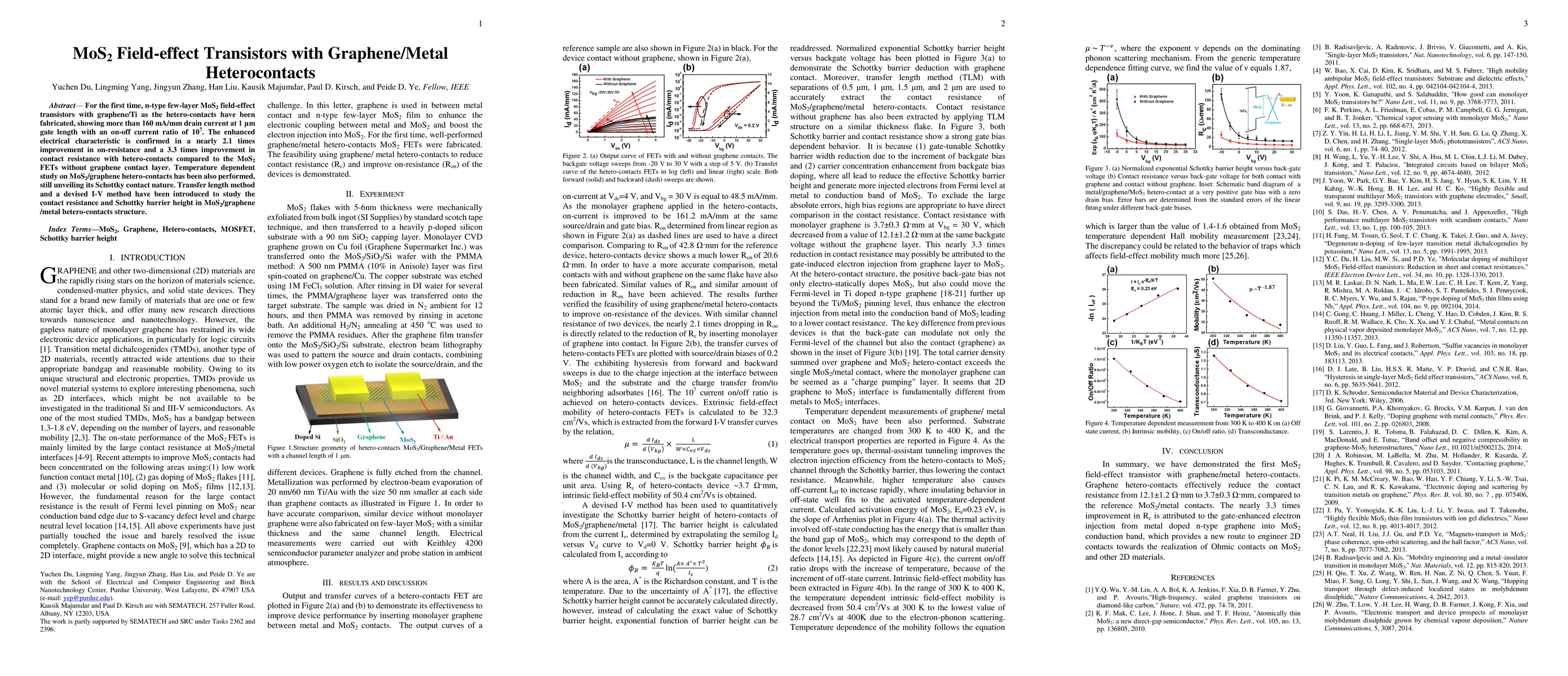
For the first time, n-type few-layer MoS2 field-effect transistors with graphene/Ti as the hetero-contacts have been fabricated, showing more than 160 mA/mm drain current at 1 {\mu}m gate length with an on-off current ratio of 107. The enhanced electrical characteristic is confirmed in a nearly 2.1 times improvement in on-resistance and a 3.3 times improvement in contact resistance with hetero-contacts compared to the MoS2 FETs without graphene contact layer. Temperature dependent study on MoS2/graphene hetero-contacts has been also performed, still unveiling its Schottky contact nature. Transfer length method and a devised I-V method have been introduced to study the contact resistance and Schottky barrier height in MoS2/graphene /metal hetero-contacts structure.
This graph shows how this paper is connected to other research. The current paper is shown in dark gray, papers that cite it are in green, and papers it references are in blue. You can:
• Hover over any node to see the paper title
• Click a node to view that paper's details
• Drag nodes to rearrange the graph
• Use the zoom controls (bottom right) to zoom in/out
Title | Authors | Year | Actions |
---|---|---|---|
Enormous Out-of-Plane Charge Rectification and Conductance through Two-Dimensional Monolayers.
|
Anthony Cabanillas, Simran Shahi, Maomao Liu, H. N. Jaiswal, Sichen Wei, Yu Fu, Anindita Chakravarty, Asma Ahmed, Xiaochi Liu, Jian Sun, Cheng Yang, Won Jong Yoo, T. Knobloch, V. Perebeinos, A. Di Bartolomeo, T. Grasser, Fei Yao, Huamin Li
|
2025
|
View Paper |
Contact engineering for two-dimensional van der Waals semiconductors
|
Jiachen Tang, Shuaixing Li, Li Zhan, Songlin Li
|
2024
|
View Paper |
Designing high-efficiency electrode contacts to two-dimensional semiconductor Cu2Se
|
Jian-chun Geng, Lei Gao, Baijin Li, Hang-Lv Zhou, Jianchen Lu, Jinming Cai
|
2023
|
View Paper |
First-principles based study of 8-Pmmn borophene and metal interface
|
Vaishnavi Vishnubhotla, S. Mitra, S. Mahapatra
|
2023
|
View Paper |
Tunable Schottky barrier of WSi2N4/graphene heterostructure via interface distance and external electric field
|
X. Ma, Huatin Bo, Xue Gong, Gang Yuan, Zhuo Peng, Jinghui Lu, Qihai Xie
|
2023
|
View Paper |
Inkjet-printed MoS2-based 3D-structured electrocatalysts on Cu films for ultra-efficient hydrogen evolution reaction
|
Pei-Zhen Li, Na Chen, A. Al-Hamry, E. Sheremet, R. Lu, Yezhou Yang, O. Kanoun, R. Baumann, R. D. Rodriguez, Jin-ju Chen
|
2023
|
View Paper |
Improvement of Visible Photodetection of Chemical Vapor Deposition-Grown MoS2 Devices via Graphene/Au Contacts
|
Yeongsik Hwa, Sang‐Soo Chee
|
2022
|
View Paper |
Electronic and Optical Properties and Device Applications for Antimonene/WS2 van der Waals Heterostructure
|
X. He, X. Deng, L. Sun, Z.H. Zhang, Z. Fan
|
2021
|
View Paper |
Thin-film electronics based on all-2D van der Waals heterostructures
|
Xinling Liu, Xiaoming Yang, Weihui Sang, Hai Huang, Wenwu Li, Yen‐Fu Lin, J. Chu
|
2021
|
View Paper |
Metal–semiconductor interface engineering in layered 2D materials for device applications
|
Monika Moun, Rajendra Singh
|
2021
|
View Paper |
SnSe field-effect transistors with improved electrical properties
|
Shuang Liu, Yujia Chen, Shengxue Yang, Chengbao Jiang
|
2021
|
View Paper |
Fabrication of Large-Area Molybdenum Disulfide Device Arrays Using Graphene/Ti Contacts
|
M. Son, Jaewon Jang, Dong Chul Kim, Seunghyup Lee, Hyo‐Soon Shin, M. Ham, Sang‐Soo Chee
|
2021
|
View Paper |
Non-invasively improving the Schottky barrier of MoS2/metal contacts by inserting a SiC layer.
|
Qinglong Fang, Xumei Zhao, Lin Yuan, Boyu Wang, C. Xia, F. Ma
|
2021
|
View Paper |
Ohmic-to-Schottky Conversion in Monolayer Tellurene–Metal Interface via Graphene Insertion
|
S. Mitra, Om Kesharwani, S. Mahapatra
|
2021
|
View Paper |
Fermi-level depinning of 2D transition metal dichalcogenide transistors
|
Ruoting Chen, Guanglong Ding, Ye Zhou, Su‐Ting Han
|
2021
|
View Paper |
Accumulation-Type Ohmic van der Waals Contacts to Nearly Intrinsic WSe2 Nanosheet-Based Channels: Implications for Field-Effect Transistors
|
Kraig Andrews, Upendra Rijal, A. Bowman, Hsun-Jen Chuang, M. Koehler, Jiaqiang Yan, D. Mandrus, Pai-Yen Chen, Zhixian Zhou
|
2021
|
View Paper |
Synthesis of Wafer‐Scale Graphene with Chemical Vapor Deposition for Electronic Device Applications
|
Bao-min Sun, Jinbo Pang, Qilin Cheng, Shu Zhang, Yufen Li, Congcong Zhang, Dehui Sun, B. Ibarlucea, Yang-qiu Li, Duo Chen, Huaimin Fan, Qingfang Han, Meng Chao, Hong Liu, Jingang Wang, G. Cuniberti, Lin Han, Weijia Zhou
|
2021
|
View Paper |
Sub‐bandgap activated charges transfer in a graphene‐MoS
2
‐graphene heterostructure
|
Sunil Kumar, Arvind Singh, A. Nivedan, Sandeep Kumar, S. Yun, Young Hee Lee, M. Tondusson, J. Degert, J. Oberlé, E. Freysz
|
2021
|
View Paper |
Direct Laser Patterning of a 2D WSe2 Logic Circuit
|
Chao Zhu, Xiaoxu Zhao, Xiaowei Wang, Jieqiong Chen, Peng Yu, Song Liu, Jiadong Zhou, Qundong Fu, Qingsheng Zeng, Yongmin He, J. Edgar, S. Pennycook, Fucai Liu, Zheng Liu
|
2021
|
View Paper |
All-2D architectures toward advanced electronic and optoelectronic devices
|
J. Yao, G. Yang
|
2021
|
View Paper |
Physics of electron emission and injection in
two‐dimensional
materials: Theory and simulation
|
Y. Ang, Liemao Cao, L. Ang
|
2021
|
View Paper |
Field-effect at electrical contacts to two-dimensional materials
|
Yao Guo, Yan Sun, A. Tang, Ching-Hua Wang, Yanqing Zhao, Mengmeng Bai, Shuting Xu, Zheqi Xu, Tao Tang, Sheng Wang, Chenguang Qiu, Kang Xu, Xubiao Peng, Junfeng Han, E. Pop, Y. Chai
|
2021
|
View Paper |
Enhanced Electrical Performance of Van der Waals Heterostructure
|
Lei Xu, Yun-Yuan Wang, C. Hsiao, I‐Chih Ni, Mei‐Hsin Chen, Chih‐I Wu
|
2021
|
View Paper |
Low-Temperature 2D/2D Ohmic Contacts in WSe2 Field-Effect Transistors as a Platform for the 2D Metal-Insulator Transition.
|
L. Stanley, Hsun-Jen Chuang, Zhixian Zhou, M. Koehler, Jiaqiang Yan, D. Mandrus, D. Popović
|
2020
|
View Paper |
Charge–Ferroelectric Transition in Ultrathin Na0.5Bi4.5Ti4O15 Flakes Probed via a Dual‐Gated Full van der Waals Transistor
|
Xiaochi Liu, Xuefan Zhou, Yuchuan Pan, Junqiang Yang, Haiyan Xiang, Yahua Yuan, Song Liu, Hang Luo, Dou Zhang, Jian Sun
|
2020
|
View Paper |
High performance complementary WS2 devices with hybrid Gr/Ni contacts.
|
Muhammad Farooq Khan, Faisal Ahmed, Shania Rehman, Imtisal Akhtar, M. A. Rehman, P. Shinde, Karim Khan, D. Kim, J. Eom, H. Lipsanen, Zhipei Sun
|
2020
|
View Paper |
Graphene based Van der Waals contacts on MoS2 field effect transistors
|
V. Mootheri, G. Arutchelvan, Sreetama Banerjee, S. Sutar, A. Leonhardt, Marie-Emmanuelle Boulon, C. Huyghebaert, M. Houssa, I. Asselberghs, I. Radu, M. Heyns, D. Lin
|
2020
|
View Paper |
An ultra-low-power and high-performance SRAM cell design based on GNRFETs
|
P. Patel, M. Malik, T. Gupta
|
2020
|
View Paper |
Research progress on the preparations, characterizations and applications of large scale 2D transition metal dichalcogenides films
|
Liwei Xiong, Kai Wang, Delong Li, Xiao-Fei Luo, J. Weng, Zhitian Liu, Han Zhang
|
2020
|
View Paper |
Tungsten Diselenide Top-gate Transistors with Multilayer Antimonene Electrodes: Gate Stacks and Epitaxially Grown 2D Material Heterostructures
|
Yu‐Wei Zhang, Jun-Yan Li, C. Wu, Chiao-Yun Chang, Shu‐Wei Chang, M. Shih, Shih-Yen Lin
|
2020
|
View Paper |
Wafer-scale production of patterned transition metal ditelluride layers for two-dimensional metal–semiconductor contacts at the Schottky–Mott limit
|
Seunguk Song, Yeoseon Sim, Se‐Yang Kim, Jung Hwa Kim, Inseon Oh, Woongki Na, Do Hee Lee, Jaewon Wang, Shili Yan, Yinan Liu, J. Kwak, Jianhao Chen, H. Cheong, Jung‐Woo Yoo, Zonghoon Lee, Soon‐Yong Kwon
|
2020
|
View Paper |
Diode‐Like Selective Enhancement of Carrier Transport through Metal–Semiconductor Interface Decorated by Monolayer Boron Nitride
|
H. N. Jaiswal, Maomao Liu, Simran Shahi, Sichen Wei, Jihea Lee, Anindita Chakravarty, Yutong Guo, Ruiqiang Wang, Jung Mu Lee, Chaoran Chang, F. Yu, R. Dixit, Xiaochi Liu, Cheng Yang, Fei Yao, Huamin Li
|
2020
|
View Paper |
A high-pressure enhanced coupling effect between graphene electrical contacts and two-dimensional materials thereby improving the performance of their constituent FET devices
|
Lijie Zhou, Chuanyang Ge, Huihui Yang, Yi Sun, Jia Zhang
|
2019
|
View Paper |
Properties of intrinsic point defects and dimers in hexagonal boron nitride
|
J. Strand, L. Larcher, A. Shluger
|
2019
|
View Paper |
Twist-angle modulation of exciton absorption in MoS2/graphene heterojunctions
|
Xiangzhe Zhang, Hang Yang, Weiwei Hou, Xiaoming Zheng, Yi Zhang, Renyan Zhang, Chuyun Deng, Xueao Zhang, S. Qin
|
2019
|
View Paper |
High Performance MoS2 N-Channel MOSFETs
|
Xiwen Liu, Zichao Ma, M. Chan, W. Liao, Lining Zhang
|
2019
|
View Paper |
Graphene surface contacts of tin disulfide transistors for switching performance improvement and contact resistance reduction
|
O. Sul, Jiyoung Bang, S. Yeom, G. Ryu, Hyung-Bin Joo, Sunjin Kim, Heewon Yang, Jusin Lee, Gunwoo Lee, Eunsuk Choi, Seung-Beck Lee
|
2019
|
View Paper |
MoTe2 Lateral Homojunction Field-Effect Transistors Fabricated using Flux-Controlled Phase Engineering.
|
Rui Ma, Huairuo Zhang, Youngdong Yoo, Zachary P DeGregorio, Lun Jin, Prafful Golani, Javad G. Azadani, T. Low, J. Johns, L. Bendersky, A. Davydov, S. Koester
|
2019
|
View Paper |
Controlling Injection Barriers for Ambipolar 2D Semiconductors via Quasi‐van der Waals Contacts
|
Junjun Wang, Feng Wang, Zhenxing Wang, Ruiqing Cheng, Lei Yin, Y. Wen, Yu Zhang, Ningning Li, Xueying Zhan, Xiangheng Xiao, Li-ping Feng, Jun He
|
2019
|
View Paper |
Phonon modes and photonic excitation transitions of MoS2 induced by top-deposited graphene revealed by Raman spectroscopy and photoluminescence
|
Yan Cao, Zhijun Wang, Q. Bian, Zhengwang Cheng, Zhibin Shao, Zongyuan Zhang, Haigen Sun, Xin Zhang, Shaojian Li, Habakubaho Gedeon, L. Liu, Xina Wang, Hui Yuan, M. Pan
|
2019
|
View Paper |
High speed mask-less laser-controlled precision micro-additive manufacture
|
J. S. Ten
|
2019
|
View Paper |
Van der Waals contacts between three-dimensional metals and two-dimensional semiconductors
|
Yan Wang, Jong Chan Kim, R. Wu, Jenny Martinez, Xiuju Song, Jieun Yang, Fang Zhao, A. Mkhoyan, H. Jeong, M. Chhowalla
|
2019
|
View Paper |
Control of the metal/WS2 contact properties using 2-dimensional buffer layers.
|
Krystian Nowakowski, R. van Bremen, H. Zandvliet, P. Bampoulis
|
2019
|
View Paper |
Understanding the transport and contact properties of metal/BN-MoS2 interfaces to realize high performance MoS2 FETs
|
J. Su, Zheng-tang Liu, Rui Guo, Jingjing Chang, Zhenhua Lin, Y. Hao
|
2019
|
View Paper |
Lowering the Schottky Barrier Height by Graphene/Ag Electrodes for High‐Mobility MoS2 Field‐Effect Transistors
|
Sang‐Soo Chee, D. Seo, H. Kim, Hanbyeol Jang, Seungmin Lee, S. Moon, Kyu Hyoung Lee, Sung Wng Kim, Hyunyong Choi, M. Ham
|
2018
|
View Paper |
Flexible integrated black phosphorus sensor arrays for high performance ion sensing
|
Peng Li, Dongzhi Zhang, Junfeng Wu, Yu-Ning Cao, Zhenling Wu
|
2018
|
View Paper |
Effective N-methyl-2-pyrrolidone wet cleaning for fabricating high-performance monolayer MoS2 transistors
|
Po-Chun Chen, Chih-Pin Lin, Chuan-Jie Hong, Chih-Hao Yang, Yun-Yan Lin, Ming-Yang Li, Lain‐Jong Li, T. Yu, C. Su, Kai-Shin Li, Y. Zhong, T. Hou, Yann-Wen Lan
|
2018
|
View Paper |
Research progress and challenges of two dimensional MoS2 field effect transistors
|
N. Divya Bharathi, K. Sivasankaran
|
2018
|
View Paper |
Charge carrier injection and transport engineering in two-dimensional transition metal dichalcogenides
|
J. D. Durán Retamal, Dharmaraj Periyanagounder, Jr-jian Ke, M. Tsai, Jr-hau He
|
2018
|
View Paper |
Progress in Contact, Doping and Mobility Engineering of MoS2: An Atomically Thin 2D Semiconductor
|
A. Rai, Hema C. P. Movva, A. Roy, D. Taneja, Sayema Chowdhury, S. Banerjee
|
2018
|
View Paper |
Gate-Controlled Large Resistance Switching Driven by Charge-Density Wave in
1T−TaS2/2H−MoS2
Heterojunctions
|
Mehak Mahajan, K. Murali, Nikhil Kawatra, K. Majumdar
|
2018
|
View Paper |
Dirac Electrons at the Source: Breaking the 60-mV/Decade Switching Limit
|
Fei Liu, Chenguang Qiu, Zhiyong Zhang, Lianmao Peng, Jian Wang, Hong Guo
|
2018
|
View Paper |
Two-dimensional transition metal dichalcogenides: interface and defect engineering.
|
Zehua Hu, Zhangting Wu, Cheng Han, Jun He, Zhenhua Ni, Wei Chen
|
2018
|
View Paper |
The growth and assembly of organic molecules and inorganic 2D materials on graphene for van der Waals heterostructures
|
Akinola D Oyedele, C. Rouleau, D. Geohegan, Kai Xiao
|
2018
|
View Paper |
High Detectivity and Transparent Few‐Layer MoS2/Glassy‐Graphene Heterostructure Photodetectors
|
Hao Xu, Xiaoyu Han, Xiao Dai, W. Liu, Jiang Wu, Juntong Zhu, Dongyoung Kim, Guifu Zou, Kimberley A Sablon, A. Sergeev, Zhengxiao Guo, Huiyun Liu
|
2018
|
View Paper |
Review of contact-resistance analysis in nano-material
|
J. Park, Jinsoo Cho, S. Jun
|
2018
|
View Paper |
Tuning electronic and optical properties of arsenene/C3N van der Waals heterostructure by vertical strain and external electric field
|
H. Zeng, Jun Zhao, A. Cheng, Lei Zhang, Zi-Hou He, Ru-Shan Chen
|
2018
|
View Paper |
Analog Circuit Applications Based on Ambipolar Graphene/MoTe2 Vertical Transistors
|
Chen Pan, Yajun Fu, Jiaxin Wang, Junwen Zeng, Guangxu Su, M. Long, Erfu Liu, Chen-Yu Wang, Anyuan Gao, Miao Wang, Yu Wang, Zhenlin Wang, S. Liang, Ru Huang, F. Miao
|
2018
|
View Paper |
Van der Waals Heterostructure Based Field Effect Transistor Application
|
Jingyu Li, Xiaozhang Chen, David-Wei Zhang, P. Zhou
|
2017
|
View Paper |
Properties of synthetic epitaxial graphene/molybdenum disulfide lateral heterostructures
|
S. Subramanian, Donna Deng, Ke Xu, Nicholas A. Simonson, Ke Wang, Kehao Zhang, Jun Li, R. Feenstra, Susan K. Fullerton‐Shirey, J. Robinson
|
2017
|
View Paper |
Promising Approach for High-Performance MoS2 Nanodevice: Doping the BN Buffer Layer to Eliminate the Schottky Barriers.
|
J. Su, Li-ping Feng, Xiaoqi Zheng, Chenlu Hu, Hongcheng Lu, Zheng-tang Liu
|
2017
|
View Paper |
Schottky Barrier Height of Pd/MoS2 Contact by Large Area Photoemission Spectroscopy.
|
H. Dong, C. Gong, R. Addou, S. McDonnell, A. Azcatl, Xiaoye Qin, Weichao Wang, Weihua Wang, C. Hinkle, R. Wallace
|
2017
|
View Paper |
Graphene‐Contacted Ultrashort Channel Monolayer MoS2 Transistors
|
Li Xie, Mengzhou Liao, Shuopei Wang, Hua Yu, Luojun Du, Jian Tang, J. Zhao, Jing Zhang, Peng Chen, Xiaobo Lu, Guole Wang, Guibai Xie, Rong Yang, D. Shi, Guangyu Zhang
|
2017
|
View Paper |
Black phosphorus transistors with van der Waals-type electrical contacts.
|
R. Quhe, Yangyang Wang, M. Ye, Qiaoxuan Zhang, Jie Yang, P. Lu, M. Lei, Jing Lu
|
2017
|
View Paper |
Vertical Charge Transport and Negative Transconductance in Multilayer Molybdenum Disulfides.
|
Yuan Liu, Jian Guo, Qiyuan He, Hao Wu, Hung-Chieh Cheng, Mengning Ding, I. Shakir, V. Gambin, Yu Huang, X. Duan
|
2017
|
View Paper |
Electrical Contacts in Monolayer Arsenene Devices.
|
Yangyang Wang, M. Ye, Mouyi Weng, Jingzhen Li, Xiuying Zhang, Han Zhang, Ying Guo, Yuanyuan Pan, Lin Xiao, Junku Liu, Feng Pan, Jing Lu
|
2017
|
View Paper |
Investigations on Field‐Effect Transistors Based on Two‐Dimensional Materials
|
T. Finge, Felix Riederer, M. Mueller, T. Grap, K. Kallis, Joachim Knoch
|
2017
|
View Paper |
Progress of Large-Scale Synthesis and Electronic Device Application of Two-Dimensional Transition Metal Dichalcogenides.
|
Xiongfei Song, Zhongxun Guo, Qiaochu Zhang, P. Zhou, W. Bao, David-Wei Zhang
|
2017
|
View Paper |
Electrical properties of graphene-metal contacts
|
T. Cusati, G. Fiori, A. Gahoi, V. Passi, M. Lemme, A. Fortunelli, G. Iannaccone
|
2017
|
View Paper |
Controlling the electronic and geometric structures of 2D insertions to realize high performance metal/insertion-MoS2 sandwich interfaces.
|
J. Su, Li-ping Feng, Wei Zeng, Zheng-tang Liu
|
2017
|
View Paper |
General solution-processed formation of porous transition-metal oxides on exfoliated molybdenum disulfides for high-performance asymmetric supercapacitors
|
Kai Wang, Y. Jing, Jixin Zhu, Le Li, L. Ying, Chao Zhang, Tianxi Liu
|
2017
|
View Paper |
Development of electronic devices based on two-dimensional materials
|
T. Das, Jong-Hyun Ahn
|
2017
|
View Paper |
Performance Evaluation and Optimization of Single Layer MoS2 Double Gate Transistors With Schottky Barrier Contacts
|
L. Zeng, Deming Zhang, Tianqi Gao, Fanghui Gong, Xiaowan Qin, Mingzhi Long, Youguang Zhang, Weisheng Zhao
|
2017
|
View Paper |
Electrically induced, non-volatile, metal insulator transition in a ferroelectric-controlled MoS2 transistor
|
Zhongyuan Lu, C. Serrao, A. Khan, J. Clarkson, Justin C. Wong, R. Ramesh, S. Salahuddin
|
2017
|
View Paper |
Doping, Contact and Interface Engineering of Two‐Dimensional Layered Transition Metal Dichalcogenides Transistors
|
Yuda Zhao, Kang Xu, Feng Pan, Changjian Zhou, F. Zhou, Y. Chai
|
2017
|
View Paper |
Work Function Tuning in Two-Dimensional MoS2 Field-Effect-Transistors with Graphene and Titanium Source-Drain Contacts
|
S. Baik, Seongil Im, H. Choi
|
2017
|
View Paper |
Angle dependence of the local electronic properties of the graphene/MoS2 interface determined by ab initio calculations
|
D. Felice, E. Abad, César González, A. Smogunov, Y. Dappe
|
2017
|
View Paper |
Optimizing Charge Injection across Transition Metal Dichalcogenide Heterojunctions: Theory and Experiment.
|
J. Guan, Hsun-Jen Chuang, Zhixian Zhou, D. Tománek
|
2017
|
View Paper |
Recent progress in high-mobility thin-film transistors based on multilayer 2D materials
|
Y. Hong, Na Liu, Demin Yin, Seongin Hong, Dong Hak Kim, Sunkook Kim, Woong Choi, Y. Yoon
|
2017
|
View Paper |
Can a Black Phosphorus Schottky Barrier Transistor Be Good Enough?
|
R. Quhe, X. Peng, Yuanyuan Pan, M. Ye, Yangyang Wang, Han Zhang, Shenyan Feng, Qiaoxuan Zhang, Jun-jie Shi, Jinbo Yang, D. Yu, M. Lei, Jing Lu
|
2017
|
View Paper |
Electric-double-layer doping of WSe2 field-effect transistors using polyethylene-oxide cesium perchlorate
|
S. Fathipour, P. Pandey, Susan K. Fullerton‐Shirey, A. Seabaugh
|
2016
|
View Paper |
Designing high performance metal-mMoS2 interfaces by two-dimensional insertions with suitable thickness.
|
J. Su, Li-ping Feng, Wei Zeng, Zheng-tang Liu
|
2016
|
View Paper |
Electronic properties of monolayer tungsten disulfide grown by chemical vapor deposition
|
Abdullah Alharbi, D. Shahrjerdi
|
2016
|
View Paper |
Pushing the Performance Limit of Sub-100 nm Molybdenum Disulfide Transistors.
|
Yuan Liu, Jian Guo, Yecun Wu, Enbo Zhu, Nathan O. Weiss, Qiyuan He, Hao Wu, Hung-Chieh Cheng, Yang Xu, I. Shakir, Yu Huang, X. Duan
|
2016
|
View Paper |
Two-dimensional semiconductors for transistors
|
M. Chhowalla, D. Jena, Hua Zhang
|
2016
|
View Paper |
Van der Waals heterostructures and devices
|
Yuan Liu, Nathan O. Weiss, Xidong Duan, Hung-Chieh Cheng, Yu Huang, X. Duan
|
2016
|
View Paper |
Atomistic modeling of the metallic-to-semiconducting phase boundaries in monolayer MoS2
|
D. Saha, S. Mahapatra
|
2016
|
View Paper |
High performance and transparent multilayer MoS2 transistors: Tuning Schottky barrier characteristics
|
Y. Hong, G. Yoo, Junyeon Kwon, Seongin Hong, W. Song, Na Liu, I. Omkaram, B. Yoo, Sanghyun Ju, Sunkook Kim, M. Oh
|
2016
|
View Paper |
Transport studies in 2D transition metal dichalcogenides and black phosphorus
|
Yuchen Du, A. Neal, Hong Zhou, P. Ye
|
2016
|
View Paper |
Computational study of interfaces and edges of 2D materials
|
M. Farmanbar
|
2016
|
View Paper |
Impact of Random Variations on Cell Stability and Write-Ability of Low-Voltage SRAMs Using Monolayer and Bilayer Transition Metal Dichalcogenide (TMD) MOSFETs
|
Chang-Hung Yu, P. Su, C. Chuang
|
2016
|
View Paper |
Effect of compression on the electronic, optical and transport properties of MoS2/graphene-based junctions
|
M. Ghorbani-Asl, P. Bristowe, K. Koziol, T. Heine, A. Kuc
|
2016
|
View Paper |
Realization of a Piezophototronic Device Based on Reduced Graphene Oxide/MoS2 Heterostructure
|
M. Javadi, S. Darbari, Y. Abdi, Farshad Ghasemi
|
2016
|
View Paper |
Field effects of current crowding in metal-MoS2 contacts
|
Hui Yuan, G. Cheng, Sheng Yu, A. Walker, C. Richter, M. Pan, Qiliang Li
|
2016
|
View Paper |
Low-Resistance 2D/2D Ohmic Contacts: A Universal Approach to High-Performance WSe2, MoS2, and MoSe2 Transistors.
|
Hsun-Jen Chuang, Bhim Chamlagain, M. Koehler, Meeghage Madusanka Perera, Jiaqiang Yan, D. Mandrus, D. Tománek, Zhixian Zhou
|
2016
|
View Paper |
Complementary Unipolar WS2 Field‐Effect Transistors Using Fermi‐Level Depinning Layers
|
Woojin Park, Yonghun Kim, U. Jung, Jin Ho Yang, C. Cho, Yun Ji Kim, Syed Mohammad Najib Hasan, Hyun Gu Kim, Han Bo Ram Lee, Byoung Hun Lee
|
2016
|
View Paper |
Thermal Transport in Single-Layer MoS2 and Black Phosphorus Transistors
|
Leitao Liu, Jing Guo
|
2016
|
View Paper |
Large-scale chemical assembly of atomically thin transistors and circuits.
|
Mervin Zhao, Yu Ye, Yimo Han, Yang Xia, Hanyu Zhu, Siqi Wang, Yuang Wang, D. Muller, Xiang Zhang
|
2015
|
View Paper |
Prospects of zero Schottky barrier height in a graphene-inserted MoS2-metal interface
|
A. Chanana, S. Mahapatra
|
2015
|
View Paper |
Electrical behavior of the Diamond layout style for MOSFETs in X-rays ionizing radiation environments
|
S. Gimenez, D. Alati
|
2015
|
View Paper |
Self-screened high performance multi-layer MoS₂ transistor formed by using a bottom graphene electrode.
|
Deshun Qu, Xiaochi Liu, Faisal Ahmed, Daeyeong Lee, W. Yoo
|
2015
|
View Paper |
Air-Stable Black Phosphorus Devices for Ion Sensing.
|
Peng Li, Dongzhi Zhang, Jingjing Liu, Hongyan Chang, Yan’e Sun, Nailiang Yin
|
2015
|
View Paper |
Electrically Tunable and Negative Schottky Barriers in Multi-layered Graphene/MoS2 Heterostructured Transistors
|
Dongri Qiu, E. Kim
|
2015
|
View Paper |
Tuning the Schottky Barrier at the Graphene/MoS2 Interface by Electron Doping: Density Functional Theory and Many-Body Calculations
|
Chengjun Jin, Filip Rasmussen, K. Thygesen
|
2015
|
View Paper |
Donor/acceptor and adsorbate effects over transport properties of Graphene Armchair Nanoribbon/MoS2 device
|
S. Shakil, S. Ahmed
|
2015
|
View Paper |
Metal-assisted chemical etching of molybdenum disulphide
|
W. Leong, J. Thong
|
2015
|
View Paper |
Air Stable Doping and Intrinsic Mobility Enhancement in Monolayer Molybdenum Disulfide by Amorphous Titanium Suboxide Encapsulation.
|
A. Rai, Amithraj Valsaraj, Hema C. P. Movva, A. Roy, R. Ghosh, S. Sonde, Sangwoo Kang, Jiwon Chang, Tanuj Trivedi, Rik Dey, S. Guchhait, S. Larentis, L. F. Register, E. Tutuc, S. Banerjee
|
2015
|
View Paper |
Highly Stable, Dual-Gated MoS2 Transistors Encapsulated by Hexagonal Boron Nitride with Gate-Controllable Contact, Resistance, and Threshold Voltage.
|
Gwan‐Hyoung Lee, X. Cui, Young Duck Kim, Ghidewon Arefe, Xian Zhang, Chul‐Ho Lee, Fan Ye, Kenji Watanabe, T. Taniguchi, P. Kim, J. Hone
|
2015
|
View Paper |
Graphene and molybdenum disulfide hybrids: synthesis and applications
|
Nanjundan Ashok Kumar, M. Dar, R. Gul, Jong‐Beom Baek
|
2015
|
View Paper |
Nb-doped single crystalline MoS2 field effect transistor
|
Saptarshi Das, M. Demarteau, A. Roelofs
|
2015
|
View Paper |
Modulation of Schottky barrier height in graphene/MoS2/metal vertical heterostructure with large current ON–OFF ratio
|
Y. Sata, R. Moriya, Takehiro Yamaguchi, Y. Inoue, Sei Morikawa, Naoto Yabuki, S. Masubuchi, T. Machida
|
2015
|
View Paper |
Large variability of contact resistance in Au/Cr/MoS2 system and its suppression by Cr thinning
|
K. Sano, Tsunaki Takahashi, K. Uchida
|
2015
|
View Paper |
Influence of metal-MoS2 interface on MoS2 transistor performance: comparison of Ag and Ti contacts.
|
Hui Yuan, G. Cheng, Lin You, Haitao Li, Hao Zhu, W. Li, J. Kopanski, Y. Obeng, A. H. Hight Walker, D. Gundlach, C. Richter, D. Ioannou, Qiliang Li
|
2014
|
View Paper |
Low resistance metal contacts to MoS2 devices with nickel-etched-graphene electrodes.
|
W. Leong, Xin Luo, Yida Li, K. Khoo, S. Y. Quek, J. Thong
|
2014
|
View Paper |
Electronics based on two-dimensional materials.
|
G. Fiori, F. Bonaccorso, G. Iannaccone, T. Palacios, D. Neumaier, A. Seabaugh, S. Banerjee, L. Colombo
|
2014
|
View Paper |
Schottky barrier heights for Au and Pd contacts to MoS2
|
Naveen Kaushik, Ankur Nipane, F. Basheer, Sudipta Dubey, S. Grover, M. Deshmukh, S. Lodha
|
2014
|
View Paper |
Contact research strategy for emerging molybdenum disulfide and other two-dimensional field-effect transistors
|
Yuchen Du, Lingming Yang, Han Liu, P. Ye
|
2014
|
View Paper |
Device perspective for black phosphorus field-effect transistors: contact resistance, ambipolar behavior, and scaling.
|
Yuchen Du, Han Liu, Yexin Deng, P. Ye
|
2014
|
View Paper |
High mobility WSe2 p- and n-type field-effect transistors contacted by highly doped graphene for low-resistance contacts.
|
Hsun-Jen Chuang, X. Tan, N. Ghimire, Meeghage Madusanka Perera, Bhim Chamlagain, M. Cheng, Jiaqiang Yan, D. Mandrus, D. Tománek, Zhixian Zhou
|
2014
|
View Paper |
Advanced contact technology
|
J. Luo, K. Jia
|
2018
|
View Paper |
Optimization of transition-metal dichalcogenides based field-effecttransistors via contact engineering
|
Meeghage Madusanka Perera
|
2016
|
View Paper |
Advances in 2D Materials for Electronic Devices
|
B. Nichols, A. Mazzoni, M. Chin, P. Shah, S. Najmaei, R. Burke, M. Dubey
|
2016
|
View Paper |
Metal Contacts on Low-Dimensional Materials
|
Huiyong Yuan
|
2014
|
View Paper |
Published: 2015-06-03
Published: 2015-06-22
Published: 2010-06-30
J. Torres, C. Bray, B. Benhamou-Bui, C. Consejo, S. S. Krishtopenko, K. Maussang, S. Ruffenach, B. Jouault, F. Teppe, Y. M. Meziani, K. Dinar, J. Delgado-Notario, E. Perez-Martin, L. Bonnet, M. Paillet, I. Rozhansky, S. Nanot
Published: 2024-11-25
Comments (0)