Summary
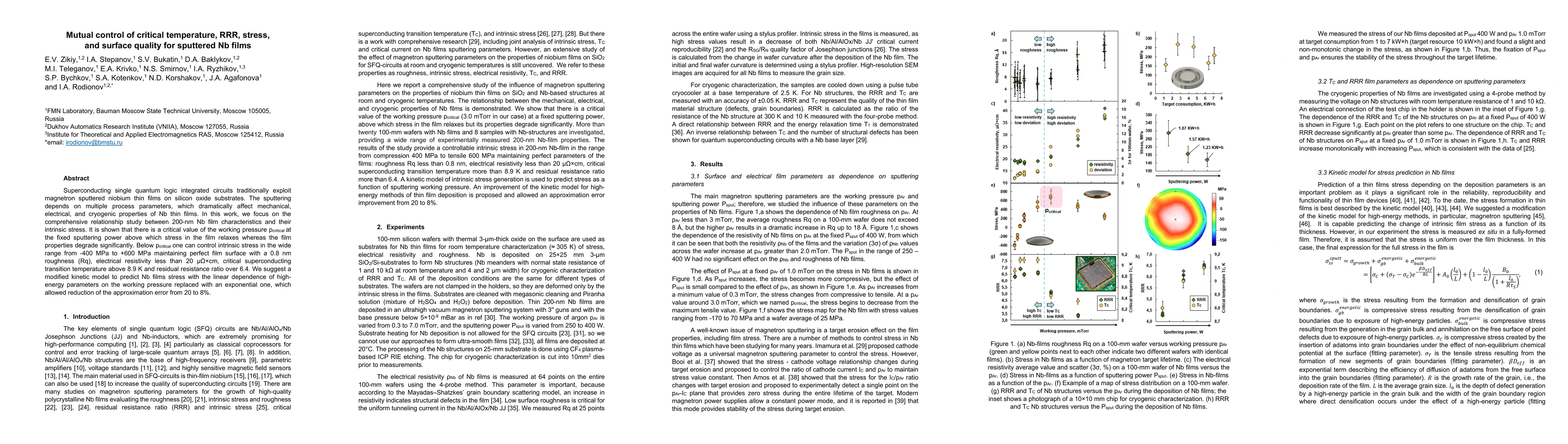
Superconducting single quantum logic integrated circuits traditionally exploit magnetron sputtered niobium thin films on silicon oxide substrates. The sputtering depends on multiple process parameters, which dramatically affect mechanical, electrical, and cryogenic properties of Nb thin films. In this work, we focus on the comprehensive relationship study between 200-nm Nb film characteristics and their intrinsic stress. It is shown that there is a critical value of the working pressure pcritical at the fixed sputtering power above which stress in the film relaxes whereas the film properties degrade significantly. Below pcritical one can control intrinsic stress in the wide range from -400 MPa to +600 MPa maintaining perfect film surface with a 0.8 nm roughness (Rq), electrical resistivity less than 20 uOhm*cm, critical superconducting transition temperature above 8.9 K and residual resistance ratio over 6.4. We suggest a modified kinetic model to predict Nb films stress with the linear dependence of high-energy parameters on the working pressure replaced with an exponential one, which allowed reduction of the approximation error from 20 to 8%.
AI Key Findings
Generated Jun 11, 2025
Methodology
The study uses magnetron sputtering to deposit 200-nm Nb films on silicon oxide substrates, varying process parameters like working pressure to analyze their impact on mechanical, electrical, and cryogenic properties.
Key Results
- A critical working pressure (pcritical) was identified at 3.0 mTorr, above which intrinsic tensile stress relaxes, but film roughness and resistivity increase, and RRR and superconducting transition temperature (TC) decrease.
- Below pcritical, intrinsic stress in Nb films can be controlled from -400 MPa to +600 MPa while maintaining perfect film surface (Rq < 0.8 nm), low electrical resistivity (< 20 μΩ×cm), high TC (> 8.9 K), and high RRR (> 6.4).
- The approximation error in predicting Nb film stress was reduced from 20% to 8% by modifying the kinetic model with exponential dependence of high-energy parameters on working pressure.
Significance
This research is crucial for optimizing the fabrication of superconducting single quantum logic integrated circuits, as it identifies the key role of working pressure in determining Nb film properties, enabling better control over critical parameters for SFQ-circuits.
Technical Contribution
The paper presents a modified kinetic model with exponential dependence on working pressure, significantly improving the approximation error for predicting Nb film stress.
Novelty
The research distinguishes itself by identifying pcritical and its impact on Nb film properties, as well as enhancing the kinetic model for improved stress prediction accuracy.
Limitations
- The study did not investigate the impact of other process parameters like sputtering power or target-to-substrate distance on film properties.
- The findings are specific to 200-nm Nb films and may not directly generalize to other thicknesses or substrate materials.
Future Work
- Further research could explore the effects of varying sputtering power and target-to-substrate distance on Nb film properties.
- Investigating the applicability of the findings to different Nb film thicknesses and substrate materials would broaden the scope of this work.
Paper Details
PDF Preview
Similar Papers
Found 4 papersNo citations found for this paper.
Comments (0)