Nanoscale electrical conductivity imaging using a nitrogen-vacancy center in diamond
Publication
Metrics
AI Quick Summary
This paper presents a nanoscale electrical conductivity imaging technique using nitrogen-vacancy centers in diamond, achieving 40-nm resolution and a 25-fold speed increase. The method monitors NV center spin relaxation to image magnetic fluctuations from thermal electron motion in metallic conductors.
Paper Preview
Abstract
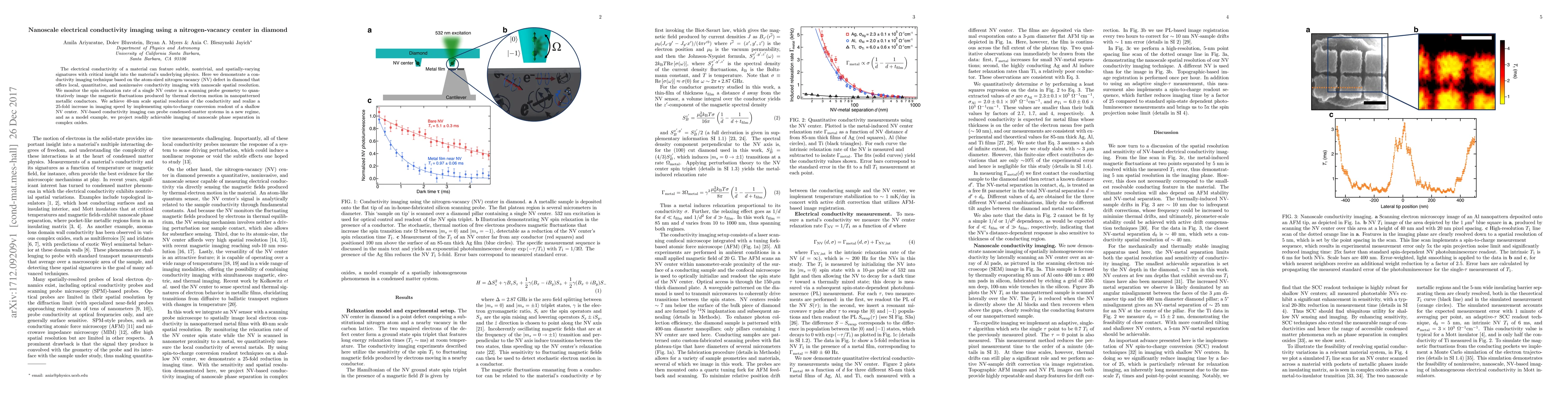
The electrical conductivity of a material can feature subtle, nontrivial, and spatially-varying signatures with critical insight into the material's underlying physics. Here we demonstrate a conductivity imaging technique based on the atom-sized nitrogen-vacancy (NV) defect in diamond that offers local, quantitative, and noninvasive conductivity imaging with nanoscale spatial resolution. We monitor the spin relaxation rate of a single NV center in a scanning probe geometry to quantitatively image the magnetic fluctuations produced by thermal electron motion in nanopatterned metallic conductors. We achieve 40-nm scale spatial resolution of the conductivity and realize a 25-fold increase in imaging speed by implementing spin-to-charge conversion readout of a shallow NV center. NV-based conductivity imaging can probe condensed-matter systems in a new regime, and as a model example, we project readily achievable imaging of nanoscale phase separation in complex oxides.
AI Key Findings
Get AI-generated insights about this paper's methodology, results, significance, and more — seven facets brought into focus.
Impact
Paper Details
PDF Preview
Key Terms
Citation Network
Current paper (gray), citations (green), references (blue)
Display is limited for performance on very large graphs.
Discussion 0