Publication
Metrics
AI Quick Summary
This study investigates the electron transport properties at graphene/pentacene interfaces, finding that the energy barrier is higher at the graphene/pentacene interface than at the pentacene/metal tip interface, attributed to the different molecular orientations of pentacene in needle-like versus dendritic structures.
Paper Preview
Abstract
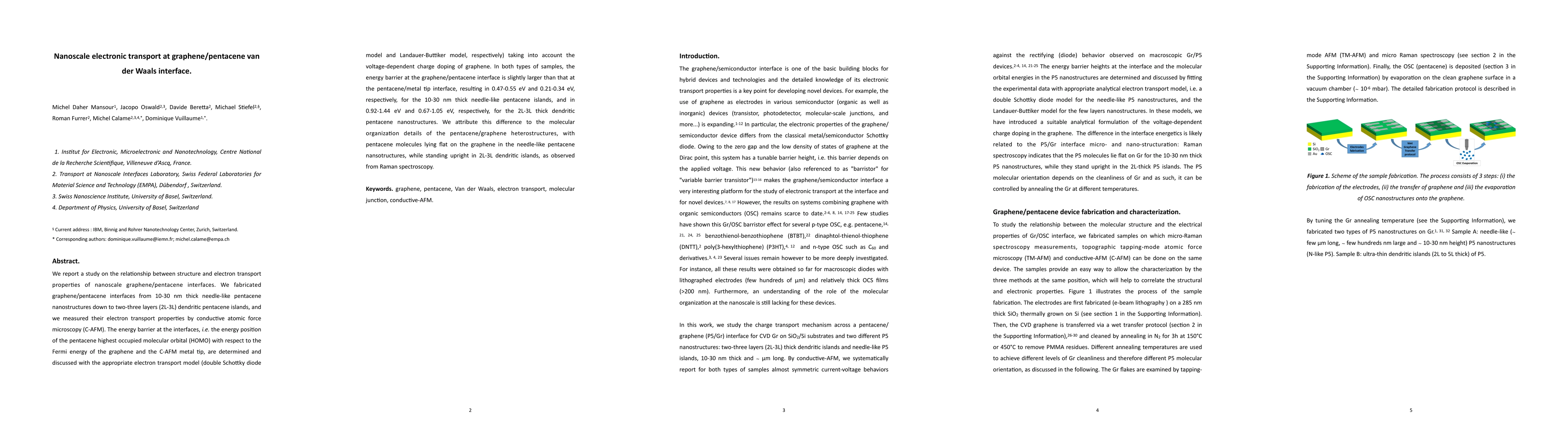
We report a study on the relationship between structure and electron transport properties of nanoscale graphene/pentacene interfaces. We fabricated graphene/pentacene interfaces from 10-30 nm thick needle-like pentacene nanostructures down to two-three layers (2L-3L) dendritic pentacene islands, and we measured their electron transport properties by conductive atomic force microscopy (C-AFM). The energy barrier at the interfaces, i.e. the energy position of the pentacene highest occupied molecular orbital (HOMO) with respect to the Fermi energy of the graphene and the C-AFM metal tip, are determined and discussed with the appropriate electron transport model (double Schottky diode model and Landauer-Buttiker model, respectively) taking into account the voltage-dependent charge doping of graphene. In both types of samples, the energy barrier at the graphene/pentacene interface is slightly larger than that at the pentacene/metal tip interface, resulting in 0.47-0.55 eV and 0.21-0.34 eV, respectively, for the 10-30 nm thick needle-like pentacene islands, and in 0.92-1.44 eV and 0.67-1.05 eV, respectively, for the 2L-3L thick dendritic pentacene nanostructures. We attribute this difference to the molecular organization details of the pentacene/graphene heterostructures, with pentacene molecules lying flat on the graphene in the needle-like pentacene nansotructures, while standing upright in 2L-3L dendritic islands, as observed from Raman spectroscopy.
AI Key Findings
Get AI-generated insights about this paper's methodology, results, significance, and more — seven facets brought into focus.
Impact
Paper Details
Authors
PDF Preview
Key Terms
Citation Network
Current paper (gray), citations (green), references (blue)
Display is limited for performance on very large graphs.
Discussion 0