Nanoscale mapping of sub-gap electroluminescence from step-bunched, oxidized 4H-SiC surfaces
Publication
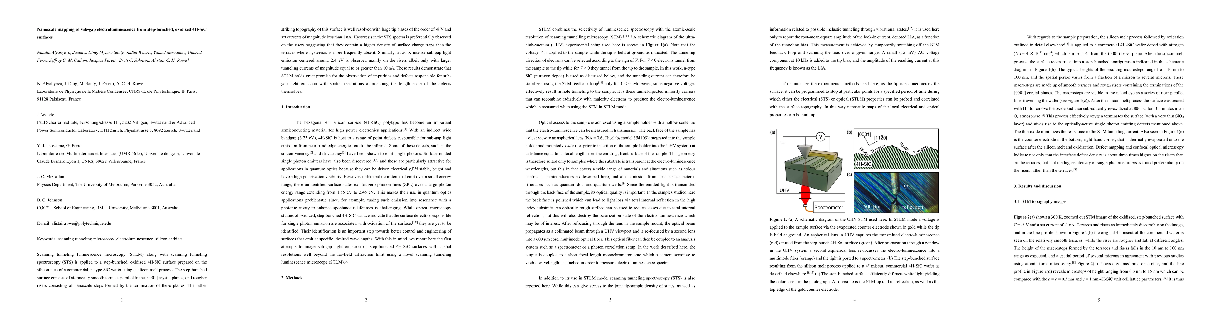
Metrics
AI Quick Summary
This study uses scanning tunneling luminescence microscopy (STLM) and scanning tunneling spectroscopy (STS) to map sub-gap electroluminescence on a step-bunched, oxidized 4H-SiC surface, revealing higher defect densities and light emission on risers compared to terraces. STLM shows promise for identifying impurities and defects with nanoscale resolution.
Paper Preview
Abstract
Scanning tunneling luminescence microscopy (STLM) along with scanning tunneling spectroscopy (STS) is applied to a step-bunched, oxidized 4H-SiC surface prepared on the silicon face of a commercial, n-type SiC wafer using a silicon melt process. The step-bunched surface consists of atomically smooth terraces parallel to the [0001] crystal planes, and rougher risers consisting of nanoscale steps formed by the termination of these planes. The rather striking topography of this surface is well resolved with large tip biases of the order of -8 V and set currents of magnitude less than 1 nA. Hysteresis in the STS spectra is preferentially observed on the risers suggesting that they contain a higher density of surface charge traps than the terraces where hysteresis is more frequently absent. Similarly, at 50 K intense sub-gap light emission centered around 2.4 eV is observed mainly on the risers albeit only with larger tunneling currents of magnitude equal to or greater than 10 nA. These results demonstrate that STLM holds great promise for the observation of impurities and defects responsible for sub-gap light emission with spatial resolutions approaching the length scale of the defects themselves.
AI Key Findings
Get AI-generated insights about this paper's methodology, results, significance, and more — seven facets brought into focus.
Impact
Paper Details
Authors
PDF Preview
Key Terms
Citation Network
Current paper (gray), citations (green), references (blue)
Display is limited for performance on very large graphs.
Discussion 0