Nanoscale optical imaging of multi-junction MoS2-WS2 lateral heterostructure
Publication
Metrics
AI Quick Summary
This paper investigates nanoscale photoluminescence characteristics of a monolayer WS2-MoS2 lateral heterostructure using plasmonic near-field tip-enhanced technology, achieving significantly higher spatial resolution than conventional methods. The study reveals enhanced photoluminescence at the hetero-interface, providing insights into the direct band gap properties of these layered semiconductors for future optoelectronic devices.
Paper Preview
Abstract
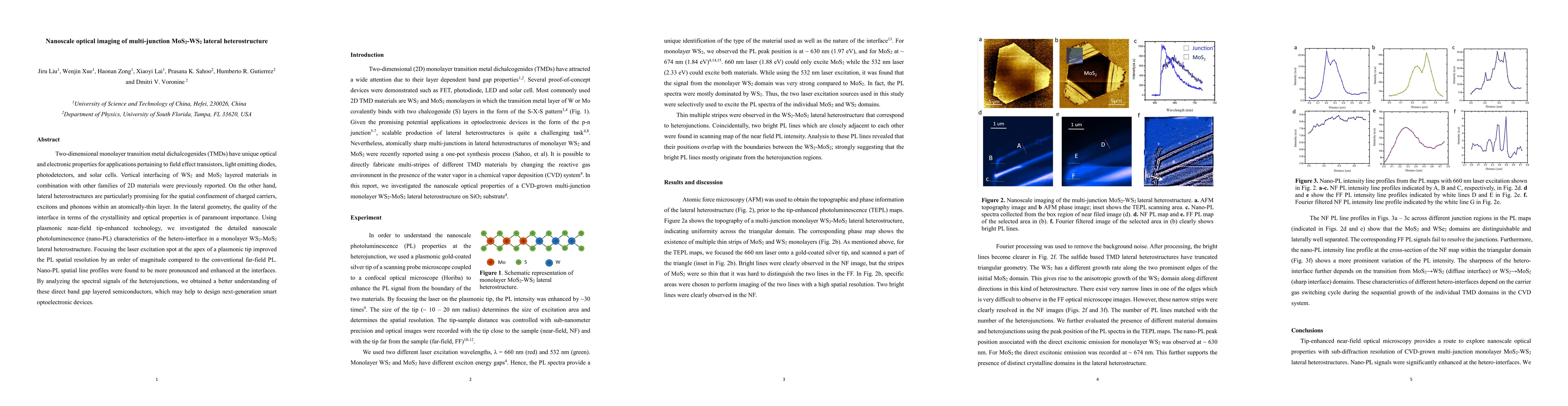
Two-dimensional monolayer transition metal dichalcogenides (TMDs) have unique optical and electronic properties for applications pertaining to field effect transistors, light emitting diodes, photodetectors, and solar cells. Vertical interfacing of WS2 and MoS2 layered materials in combination with other families of 2D materials were previously reported. On the other hand, lateral heterostructures are particularly promising for the spatial confinement of charged carriers, excitons and phonons within an atomically-thin layer. In the lateral geometry, the quality of the interface in terms of the crystallinity and optical properties is of paramount importance. Using plasmonic near-field tip-enhanced technology, we investigated the detailed nanoscale photoluminescence (nano-PL) characteristics of the hetero-interface in a monolayer WS2-MoS2 lateral heterostructure. Focusing the laser excitation spot at the apex of a plasmonic tip improved the PL spatial resolution by an order of magnitude compared to the conventional far-field PL. Nano-PL spatial line profiles were found to be more pronounced and enhanced at the interfaces. By analyzing the spectral signals of the heterojunctions, we obtained a better understanding of these direct band gap layered semiconductors, which may help to design next-generation smart optoelectronic devices.
AI Key Findings
Get AI-generated insights about this paper's methodology, results, significance, and more — seven facets brought into focus.
Impact
Paper Details
PDF Preview
Key Terms
Citation Network
Current paper (gray), citations (green), references (blue)
Display is limited for performance on very large graphs.
Discussion 0