Publication
Metrics
Paper Preview
Abstract
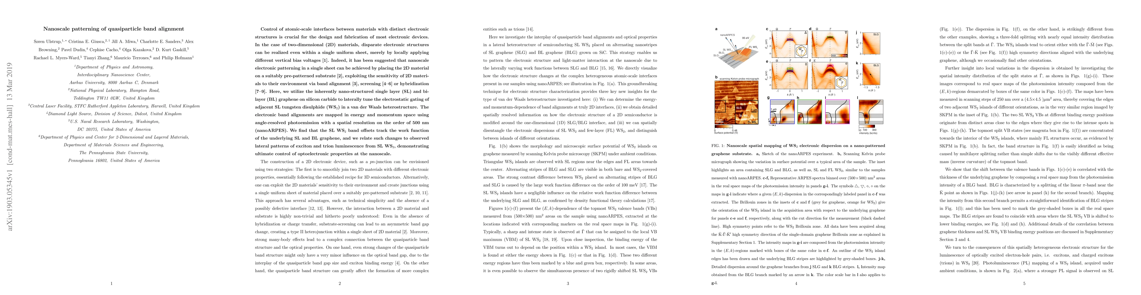
Control of atomic-scale interfaces between materials with distinct electronic structures is crucial for the design and fabrication of most electronic devices. In the case of two-dimensional (2D) materials, disparate electronic structures can be realized even within a single uniform sheet, merely by locally applying different vertical bias voltages. Indeed, it has been suggested that nanoscale electronic patterning in a single sheet can be achieved by placing the 2D material on a suitably pre-patterned substrate, exploiting the sensitivity of 2D materials to their environment via band alignment, screening or hybridization. Here, we utilize the inherently nano-structured single layer (SL) and bilayer (BL) graphene on silicon carbide to laterally tune the electrostatic gating of adjacent SL tungsten disulphide (WS$_2$) in a van der Waals heterostructure. The electronic band alignments are mapped in energy and momentum space using angle-resolved photoemission with a spatial resolution on the order of 500~nm (nanoARPES). We find that the SL WS$_2$ band offsets track the work function of the underlying SL and BL graphene, and we relate such changes to observed lateral patterns of exciton and trion luminescence from SL WS$_2$, demonstrating ultimate control of optoelectronic properties at the nanoscale.
AI Key Findings
Get AI-generated insights about this paper's methodology, results, significance, and more — seven facets brought into focus.
Impact
Paper Details
Authors
PDF Preview
Key Terms
Citation Network
Current paper (gray), citations (green), references (blue)
Display is limited for performance on very large graphs.
Discussion 0