Nanostructure engineering of epitaxial piezoelectric {\alpha}-quartz thin films on silicon
Publication
Metrics
AI Quick Summary
The paper reports the successful fabrication of large-scale, ordered arrays of epitaxial piezoelectric quartz nanostructures on silicon substrates using a combination of advanced lithographic techniques. These nanostructures, maintaining their crystallinity and piezoelectric properties, pave the way for advanced GHz frequency telecommunication devices and high-sensitivity sensors.
Paper Preview
Abstract
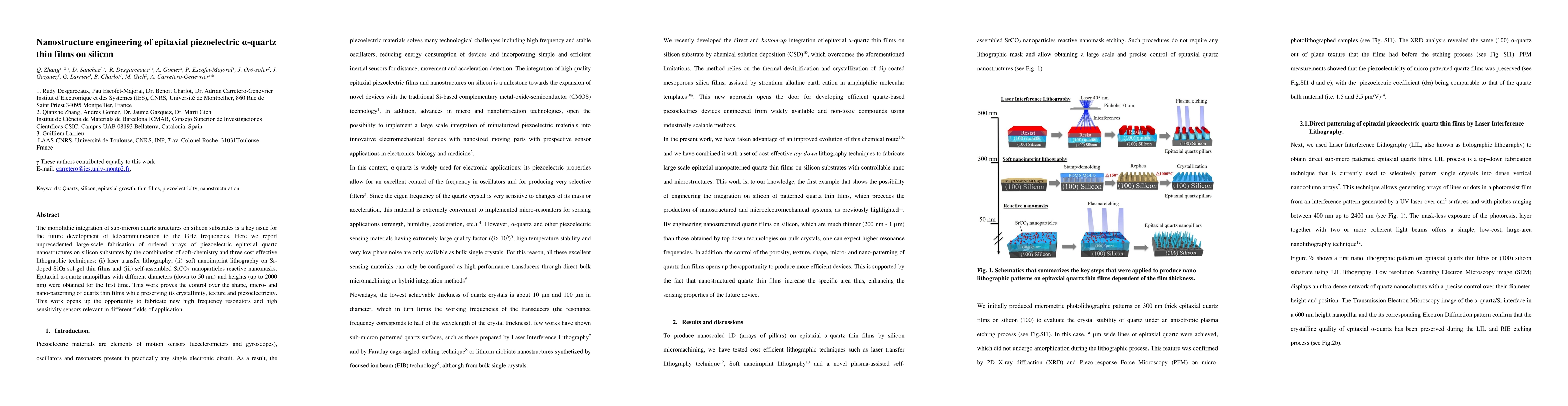
The monolithic integration of sub-micron quartz structures on silicon substrates is a key issue for the future development of telecommunication to the GHz frequencies. Here we report unprecedented large-scale fabrication of ordered arrays of piezoelectric epitaxial quartz nanostructures on silicon substrates by the combination of soft-chemistry and three cost effective lithographic techniques: (i) laser transfer lithography, (ii) soft nanoimprint lithography on Sr-doped SiO2 sol-gel thin films and (iii) self-assembled SrCO3 nanoparticles reactive nanomasks. Epitaxial {\alpha}-quartz nanopillars with different diameters (down to 50 nm) and heights (up to 2000 nm) were obtained for the first time. This work proves the control over the shape, micro- and nano-patterning of quartz thin films while preserving its crystallinity, texture and piezoelectricity. This work opens up the opportunity to fabricate new high frequency resonators and high sensitivity sensors relevant in different fields of application.
AI Key Findings
Get AI-generated insights about this paper's methodology, results, significance, and more — seven facets brought into focus.
Impact
Paper Details
Authors
PDF Preview
Key Terms
Citation Network
Current paper (gray), citations (green), references (blue)
Display is limited for performance on very large graphs.
Discussion 0