01
MethodologyHow they did it
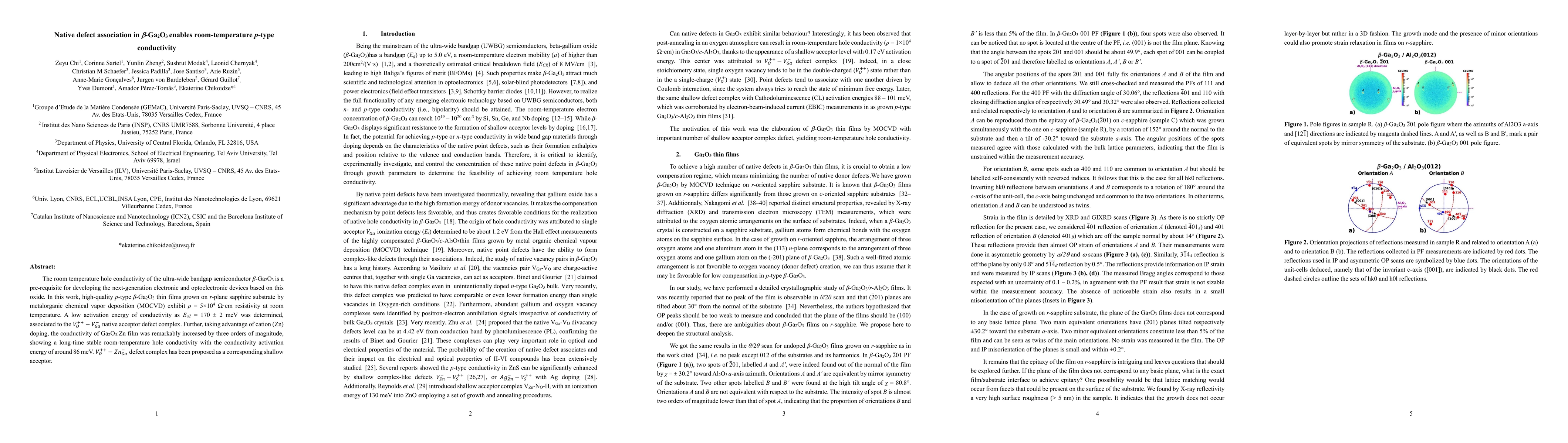
The research utilized metalorganic chemical vapor deposition (MOCVD) to grow high-quality p-type beta-Ga2O3 thin films on r-plane sapphire substrates, followed by characterization using techniques such as secondary-ion mass spectroscopy (SIMS), X-ray diffraction (XRD), optical transmittance/reflectance measurements, Raman spectroscopy, X-ray photoemission spectroscopy (XPS), cathodoluminescence (CL), and Hall effect measurements.
Discussion 0