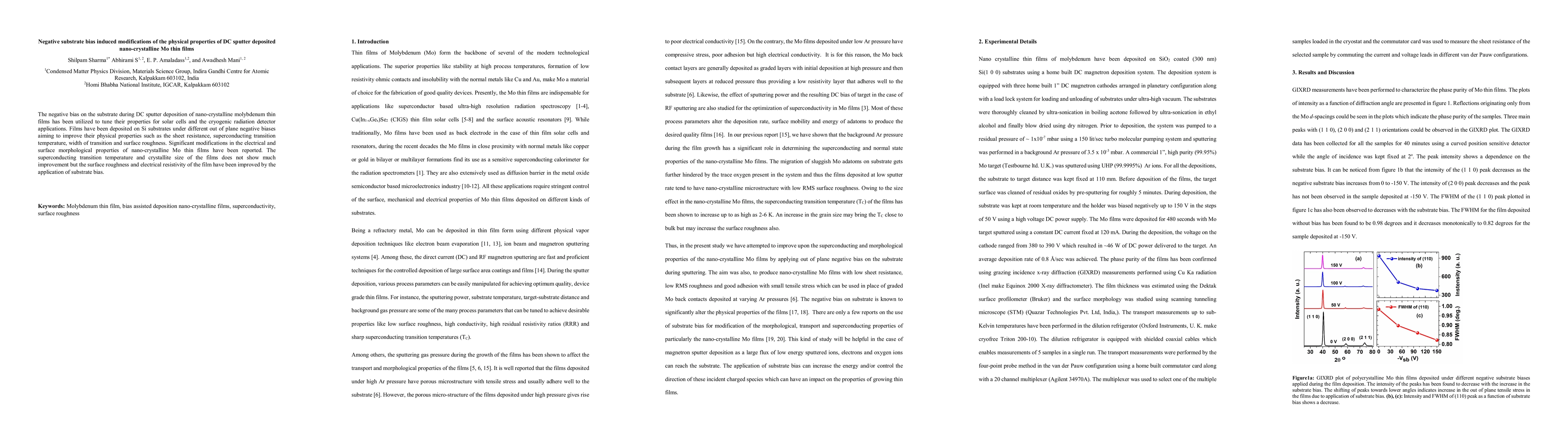
Effect of Substrate Bias on the Structural and Electrical Properties of Sputtered Mo Thin Films on Flexible Substrates
|
Jiaxiong Xu
|
2016
|
View Paper
|
Synthesis and characterization of DC magnetron sputtered nano structured molybdenum thin films
|
Sachin R. Rondiya, Avinash V. Rokade, A. Jadhavar, Subhash M. Pandharkar, R. Kulkarni, Smita Karpe, K. Diwate, S. Jadkar
|
2016
|
View Paper
|
Review of superconducting transition-edge sensors for x-ray and gamma-ray spectroscopy
|
J. Ullom, D. Bennett
|
2015
|
View Paper
|
Preparation and Characterization of Molybdenum Thin Films by Direct-Current Magnetron Sputtering
|
Shih-Fan Chen, Shea-Jue Wang, Win-Der Lee, Ming-Hong Chen, Chao-Nan Wei, H. Bor
|
2015
|
View Paper
|
Enhanced superconductivity and superconductor to insulator transition in nano-crystalline molybdenum thin films
|
Shilpam Sharma, E. Amaladass, N. Sharma, V. Harimohan, S. Amirthapandian, A. Mani
|
2015
|
View Paper
|
Molybdenum deposited on Si (111), SiO2, and amorphous Si through RF magnetron sputtering
|
X. Jiao, Jie Yang, Rui Zhang, N. Zhang, H. Zhong, Yu Shi
|
2014
|
View Paper
|
Deposition and characterization of molybdenum thin films using dc-plasma magnetron sputtering
|
Majid Khan, M. Islam
|
2013
|
View Paper
|
NIH Image to ImageJ: 25 years of image analysis
|
C. Schneider, W. Rasband, K. Eliceiri
|
2012
|
View Paper
|
Size and dimensionality effects in superconducting Mo thin films
|
L. Fàbrega, A. Camón, I. Fernández-Martínez, J. Sesé, M. Parra-Borderías, O. Gil, R. González-Arrabal, J. L. Costa-Krämer, F. Briones
|
2011
|
View Paper
|
Optimization of molybdenum thin films for electrodeposited CIGS solar cells
|
M. Jubault, L. Ribeaucourt, E. Chassaing, G. Renou, D. Lincot, F. Donsanti
|
2011
|
View Paper
|
Preparation and characterization of DC sputtered molybdenum thin films
|
A. Kashyout, H. Soliman, H. A. Gabal, Poussy Aly Ibrahim, M. Fathy
|
2011
|
View Paper
|
Effects of Stress and Morphology on the Resistivity and Critical Temperature of Room-Temperature-Sputtered Mo Thin Films
|
L. Fàbrega, I. Fernández-Martínez, M. Parra-Borderías, O. Gil, A. Camón, R. González-Arrabal, J. Sesé, J. Santiso, J. Costa-Kramer, F. Briones
|
2009
|
View Paper
|
Large-Area Microcalorimeter Detectors for Ultra-High-Resolution X-Ray and Gamma-Ray Spectroscopy
|
M. Bacrania, A. Hoover, P. Karpius, M. Rabin, C. Rudy, D. Vo, J. Beall, D. Bennett, W. Doriese, G. Hilton, R. Horansky, K. Irwin, N. Jethava, E. Sassi, J. Ullom, L. Vale
|
2009
|
View Paper
|
The effect of deposition parameters on radiofrequency sputtered molybdenum thin films
|
H. Khatri, S. Marsillac
|
2008
|
View Paper
|
WSXM: a software for scanning probe microscopy and a tool for nanotechnology.
|
I. Horcas, R. Fernandez, J. Gómez‐Rodríguez, J. Colchero, J. Gómez‐Herrero, A. Baró
|
2007
|
View Paper
|
Stress
|
R. Hayward
|
2005
|
View Paper
|
Study of the Mo thin films and Mo/CIGS interface properties
|
L. Assmann, J. Bernède, A. Drici, C. Amory, E. Halgand, M. Morsli
|
2005
|
View Paper
|
Effect of r.f.-sputtered Mo substrate on the microstructure of electrodeposited CuInSe2 thin films
|
M. Martínez, C. Guillén
|
1998
|
View Paper
|
Sputtered molybdenum bilayer back contact for copper indium diselenide-based polycrystalline thin-film solar cells
|
J. Scofield, A. Duda, D. Albin, B. Ballard, P. Predecki
|
1995
|
View Paper
|
The effect of ion bombardment on the microstructure and properties of molybdenum films
|
R. Hoffman, J. C. Lin, J. Chambers
|
1991
|
View Paper
|
Stress, strain, and microstructure of sputter‐deposited Mo thin films
|
T. J. Vink, M. Somers, J. Daams, A. Dirks
|
1991
|
View Paper
|
Effects of Oxygen on the Properties of Sputtered Molybdenum Thin Films
|
T. Yamaguchi, R. Miyagawa
|
1991
|
View Paper
|
The effects of oxygen concentration in sputter-deposited molybdenum films
|
T. Bardin, J. G. Pronkoz, R. Budhani, J. Lin, R. Bunshah
|
1988
|
View Paper
|
Effects of substrate bias on the resistivity and microstructure of molybdenum and molybdenum silicide films
|
J. Lin, R. Budhani, R. Bunshah
|
1987
|
View Paper
|
Electrical resistivity of vaccum‐deposited molybdenum films
|
H. Oikawa, T. Tsuchiya
|
1978
|
View Paper
|
Effect of heat treatment after deposition on internal stress in molybdenum films on SiO2/Si substrates
|
H. Oikawa, Y. Nakajima
|
1977
|
View Paper
|
High temperature X-ray metallography: I. A new debye-scherrer camera for use at very high temperatures II. A new parafocusing camera III. Applications to the study of chromium, hafnium, molybdenum, rhodium, ruthenium and tungsten
|
R. G. Ross, W. Hume-rothery
|
1963
|
View Paper
|
Data for Paper: The Impact of Substrate Bias on a Remote Plasma Sputter Coating Process for Conformal Coverage of Trenches and 3D Structures
|
Hayley Brown
|
2015
|
View Paper
|
Handbook of sputter deposition technology : fundamentals and applications for functional thin films, nanomaterials and MEMS
|
K. Wasa, I. Kanno, H. Kotera
|
2012
|
View Paper
|
Observation of sharp resistance anomalies near Tc in granular superconductors
|
S. Rubin, T. Schimpfke, B. Weitzel, C. Vossloh, H. Micklitz
|
1992
|
View Paper
|
Handbook of sputter deposition technology
|
K. Wasa, S. Hayakawa
|
1992
|
View Paper
|
Handbook of plasma processing technology: Fundamentals, etching, deposition and surface interactions
|
W. Steckelmacher
|
1991
|
View Paper
|
Handbook of Sputter Deposition Technology: Fundamentals and Applications for Functional Thin Films, Nano-Materials and MEMS, Elsevier Science2012
|
|
2012
|
|
Molybdenum deposited on Si (111)
|
|
2014
|
|
High temperature X-ray metallography: I
|
|
1963
|
|
SiO2, and amorphous Si through RF magnetron sputtering
|
|
2014
|
|
Comments (0)