This study explores how non-uniform strain fields affect excitons in WS$_2$ monolayers, revealing peak shifts and spectral changes indicative of increased free electron density and conversion of neutral excitons to trions. Non-uniform strain engineering emerges as a valuable tool for tuning the optoelectronic properties of two-dimensional semiconductors.
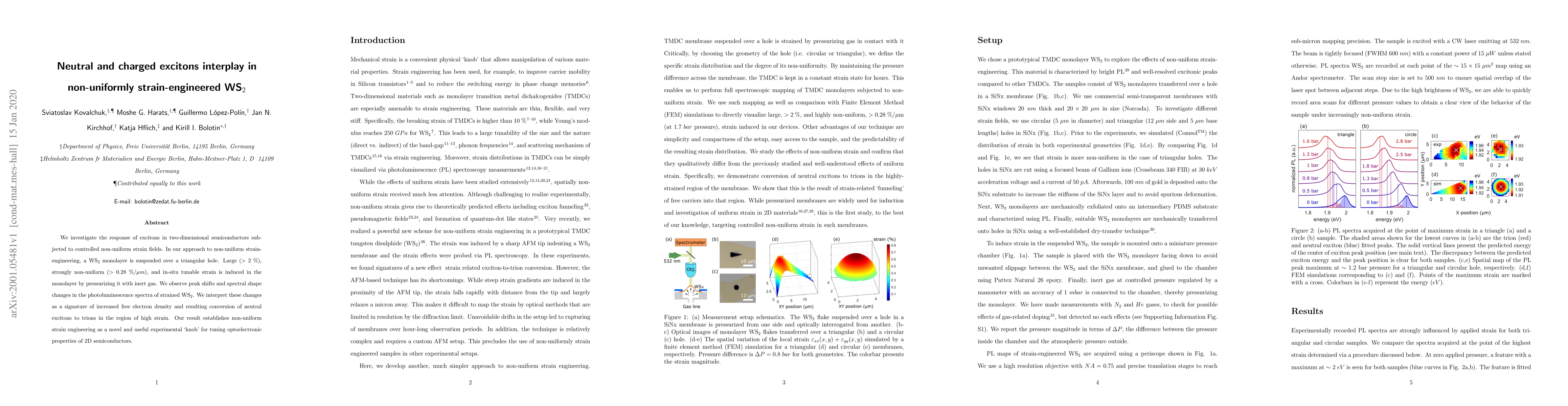
We investigate the response of excitons in two-dimensional semiconductors subjected to controlled non-uniform strain fields. In our approach to non-uniform strain-engineering, a WS$_2$ monolayer is suspended over a triangular hole. Large ($>2\;\%$), strongly non-uniform ($>0.28\;\%/\mu m$), and in-situ tunable strain is induced in the monolayer by pressurizing it with inert gas. We observe peak shifts and spectral shape changes in the photoluminescence spectra of strained WS$_2$. We interpret these changes as a signature of increased free electron density and resulting conversion of neutral excitons to trions in the region of high strain. Our result establishes non-uniform strain engineering as a novel and useful experimental `knob' for tuning optoelectronic properties of 2D semiconductors.
This graph shows how this paper is connected to other research. The current paper is shown in dark gray, papers that cite it are in green, and papers it references are in blue. You can:
• Hover over any node to see the paper title
• Click a node to view that paper's details
• Drag nodes to rearrange the graph
• Use the zoom controls (bottom right) to zoom in/out
Title | Authors | Year | Actions |
---|---|---|---|
Strain fingerprinting of exciton valley character in 2D semiconductors
|
Abhijeet M. Kumar, D. Yagodkin, Roberto Rosati, Douglas J Bock, C. Schattauer, Sarah Tobisch, Joakim Hagel, Bianca Höfer, J. N. Kirchhof, Pablo Hernández López, Kenneth Burfeindt, Sebastian Heeg, Cornelius Gahl, F. Libisch, E. Malic, K. Bolotin
|
2024
|
View Paper |
Strain distribution in WS2 monolayers detected through polarization-resolved second harmonic generation
|
G. Kourmoulakis, S. Psilodimitrakopoulos, G. Maragkakis, L. Mouchliadis, A. Michail, J. Christodoulides, Manoj Tripathi, Alan B. Dalton, J. Parthenios, K. Papagelis, Emmanuel Stratakis, G. Kioseoglou
|
2024
|
View Paper |
Fine-Tuning of the Excitonic Response in Monolayer WS2 Domes via Coupled Pressure and Strain Variation.
|
E. Stellino, B. D'Alò, E. Blundo, Paolo Postorino, A. Polimeni
|
2024
|
View Paper |
Strain control of hybridization between dark and localized excitons in a 2D semiconductor
|
Pablo Hernández López, Sebastian Heeg, C. Schattauer, S. Kovalchuk, Abhijeet Kumar, Douglas J Bock, J. N. Kirchhof, B. Höfer, K. Greben, D. Yagodkin, L. Linhart, F. Libisch, K. Bolotin
|
2022
|
View Paper |
Mechanically-tunable bandgap closing in 2D graphene phononic crystals
|
J. N. Kirchhof, K. Bolotin
|
2022
|
View Paper |
Non‐Uniform Strain Engineering of 2D Materials
|
S. Kovalchuk, J. N. Kirchhof, K. Bolotin, Moshe G. Harats
|
2022
|
View Paper |
Enhanced Dielectric Screening and Photoluminescence from Nanopillar-Strained MoS2 Nanosheets: Implications for Strain Funneling in Optoelectronic Applications
|
Mounika Vutukuru, H. Ardekani, Zhuofa Chen, R. Wilmington, K. Gundogdu, A. Swan
|
2021
|
View Paper |
Spatiotemporally controlled room-temperature exciton transport under dynamic strain
|
Kanak Datta, Zheng Lyu, Zidong Li, T. Taniguchi, Kenji Watanabe, P. Deotare
|
2021
|
View Paper |
Strain-tuning of the electronic, optical, and vibrational properties of two-dimensional crystals
|
E. Blundo, E. Cappelluti, M. Felici, G. Pettinari, A. Polimeni
|
2021
|
View Paper |
Limits of funneling efficiency in non-uniformly strained 2D semiconductors
|
Moshe G. Harats, K. Bolotin
|
2020
|
View Paper |
Published: 2020-05-20
Suman Chatterjee, Ivan Timokhin, Artem Mishchenko, Gokul M. A., Atikur Rahman, Sagnik Chatterjee, Kausik Majumdar, Tamaghna Chowdhury, Pablo Díaz Núñez, Prasenjit Ghosh, Dibyasankar Das
Published: 2023-12-27
Published: 2024-02-19
Comments (0)