Reaching lasing in electrically pumped microdevices based on
solution-processed semiconductors poses a major scientific and technological
challenge. Halide perovskites offer a promising platform for electrical
injection, since their optically excited single-crystal cavities and
predesigned or postprocessed microstructures have exhibited low lasing
threshold. Indirect electrical pumping of a dual-cavity perovskite laser was
recently obtained, utilizing a well-established technological concept of
embedding a high-luminosity light-emitting diode (LED) with a high-gain medium
into an integrated device. Direct charge-carrier injection into a perovskite
LED excited by auxiliary short-, optical-pulses resulted into amplified
spontaneous emission. Other efforts for rational engineering of architectures
that allow for high charge-carrier density are still to demonstrate lasing.
Here, we develop a novel strategy for achieving direct electrical pumping of a
perovskite laser. We integrate a solution-grown CsPbBr3 microplate with
chemically inert single-walled carbon nanotube electrodes and embed them into
an optical microcavity. By cooling the microdevice down to 8 K at a constant
current, a perovskite p-i-n diode is formed that facilitates a balanced carrier
injection at high current densities. The perovskite microcavity diode operates
in the strong coupling regime, exhibiting polariton lasing under a direct
current of 65 uA.
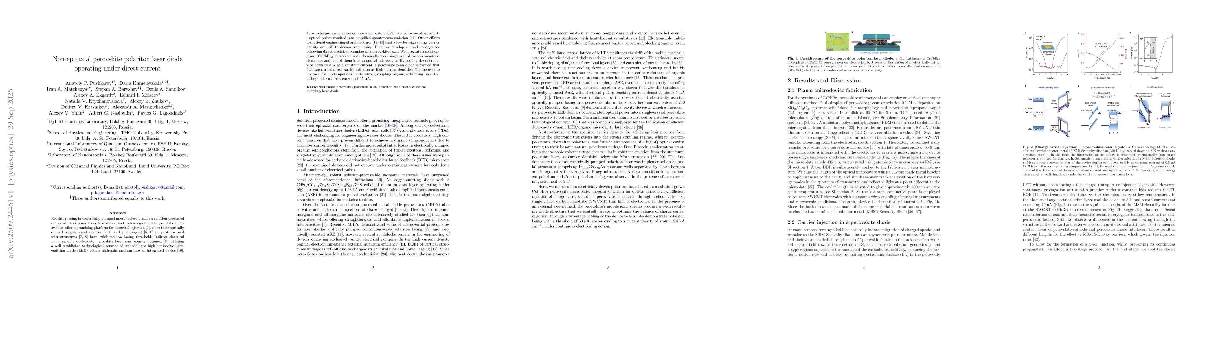
Discussion 0