Publication
Metrics
AI Quick Summary
This paper investigates spin transport in ferromagnet/semiconductor Schottky contacts with non-linear and rectifying electrical transport. It finds that non-linear effects reduce spin detection sensitivity and increase back-flow, requiring higher contact resistance to avoid it, while enabling spin detection via non-magnetic metal contacts.
Paper Preview
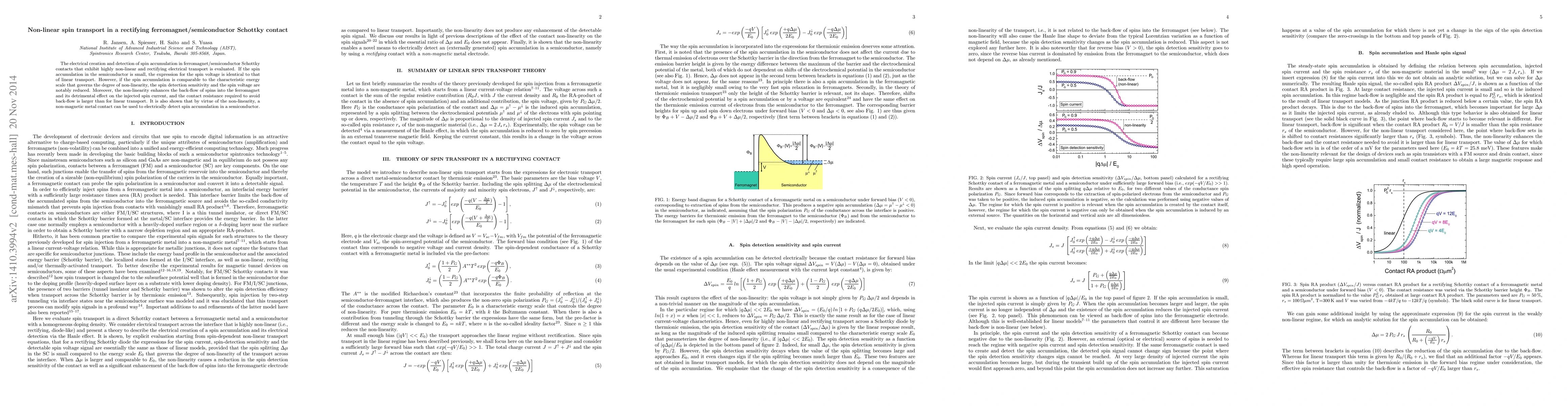
Abstract
The electrical creation and detection of spin accumulation in ferromagnet/semiconductor Schottky contacts that exhibit highly non-linear and rectifying electrical transport is evaluated. If the spin accumulation in the semiconductor is small, the expression for the spin voltage is identical to that of linear transport. However, if the spin accumulation is comparable to the characteristic energy scale that governs the degree of non-linearity, the spin detection sensitivity and the spin voltage are notably reduced. Moreover, the non-linearity enhances the back-flow of spins into the ferromagnet and its detrimental effect on the injected spin current, and the contact resistance required to avoid back-flow is larger than for linear transport. It is also shown that by virtue of the non-linearity, a non-magnetic metal contact can be used to electrically detect spin accumulation in a semiconductor.
AI Key Findings
Get AI-generated insights about this paper's methodology, results, significance, and more — seven facets brought into focus.
Impact
Paper Details
PDF Preview
Key Terms
Citation Network
Current paper (gray), citations (green), references (blue)
Display is limited for performance on very large graphs.
Discussion 0