01
MethodologyHow they did it
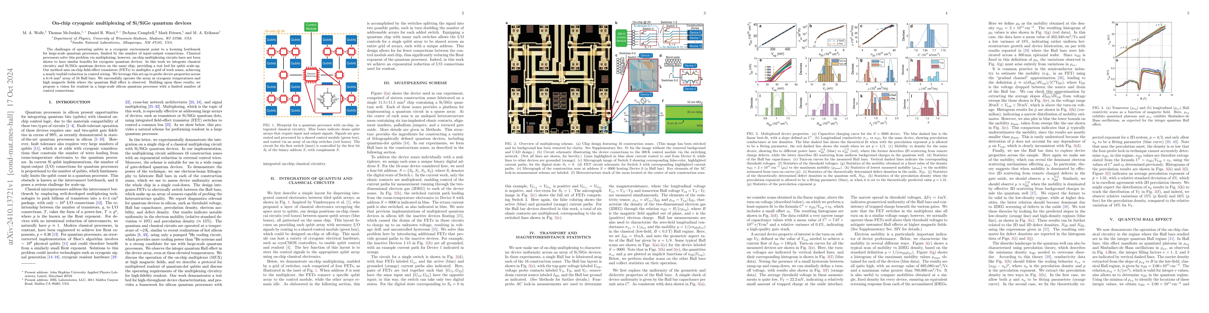
The research integrates classical circuitry with Si/SiGe quantum devices on the same chip, using on-chip FETs for multiplexing a grid of work zones, achieving a nearly tenfold reduction in control wiring. This setup allows for probing device properties across a 6x6mm² array of 16 Hall bars at cryogenic temperatures and high magnetic fields where the quantum Hall effect is observed.
Discussion 0