Publication
Metrics
AI Quick Summary
This paper introduces 1D van der Waals heterostructures, coaxially stacked nanotubes comprising an inner conductive CNT, a middle insulating BNNT, and an outer semiconducting MoS2 nanotube. The method demonstrates potential for creating versatile semiconducting nanotube materials.
Paper Preview
Abstract
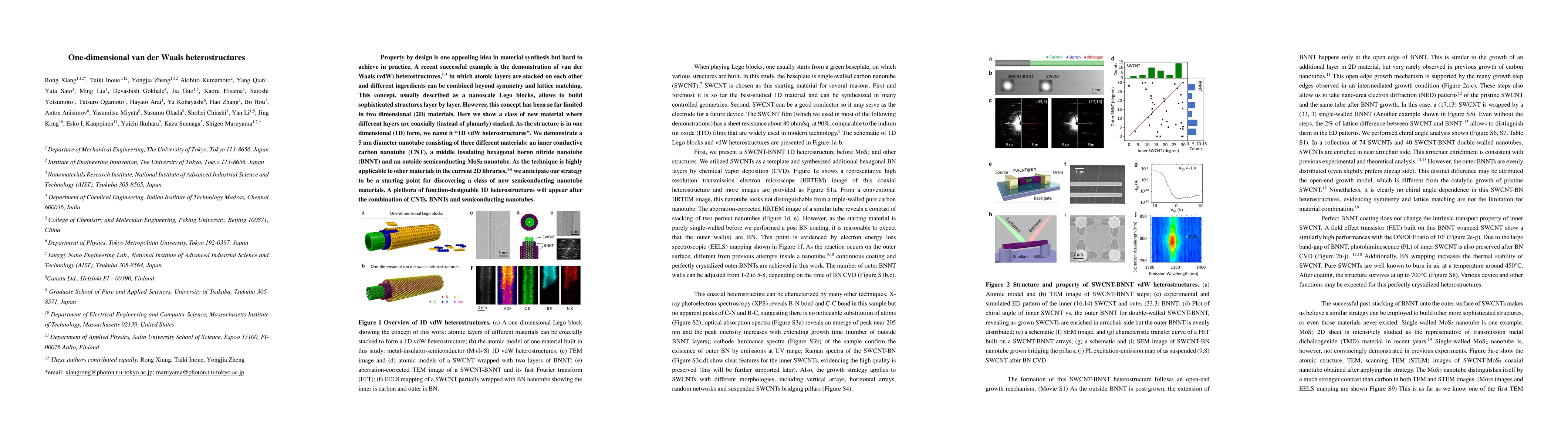
Property by design is one appealing idea in material synthesis but hard to achieve in practice. A recent successful example is the demonstration of van der Waals (vdW) heterostructures,1-3 in which atomic layers are stacked on each other and different ingredients can be combined beyond symmetry and lattice matching. This concept, usually described as a nanoscale Lego blocks, allows to build sophisticated structures layer by layer. However, this concept has been so far limited in two dimensional (2D) materials. Here we show a class of new material where different layers are coaxially (instead of planarly) stacked. As the structure is in one dimensional (1D) form, we name it "1D vdW heterostructures". We demonstrate a 5 nm diameter nanotube consisting of three different materials: an inner conductive carbon nanotube (CNT), a middle insulating hexagonal boron nitride nanotube (BNNT) and an outside semiconducting MoS2 nanotube. As the technique is highly applicable to other materials in the current 2D libraries,4-6 we anticipate our strategy to be a starting point for discovering a class of new semiconducting nanotube materials. A plethora of function-designable 1D heterostructures will appear after the combination of CNTs, BNNTs and semiconducting nanotubes.
AI Key Findings
Get AI-generated insights about this paper's methodology, results, significance, and more — seven facets brought into focus.
Impact
Paper Details
Authors
PDF Preview
Key Terms
Citation Network
Current paper (gray), citations (green), references (blue)
Display is limited for performance on very large graphs.
Discussion 0