Summary
GaN/SiO2 core/shell nanowires are grown by cobalt phthalocyanine catalyst assisted vapor-liquid-solid route, in which Si wafer coated with a mixture of gallium and indium is used as the source for Ga and Si and ammonia is used as the precursor for nitrogen and hydrogen. Gallium in the presence of indium and hydrogen, which results from the dissociation of ammonia, forms Si-Ga-In alloy at the growth temperature around 910 degree Celsius. This alloy acts as the source of Si, Ga and In. A detailed study using a variety of characterization tools reveals that these wires, which are several tens of micron long, has a diameter distribution of the core ranging from 20 to 50 nm, while the thickness of the amorphous SiO2 shell layer is about 10 nm. These wires grow along direction. It has also been observed that the average width of these wires decreases, while their density increases as the gallium proportion in the Ga-In mixture is increased.
AI Key Findings
Get AI-generated insights about this paper's methodology, results, and significance.
Paper Details
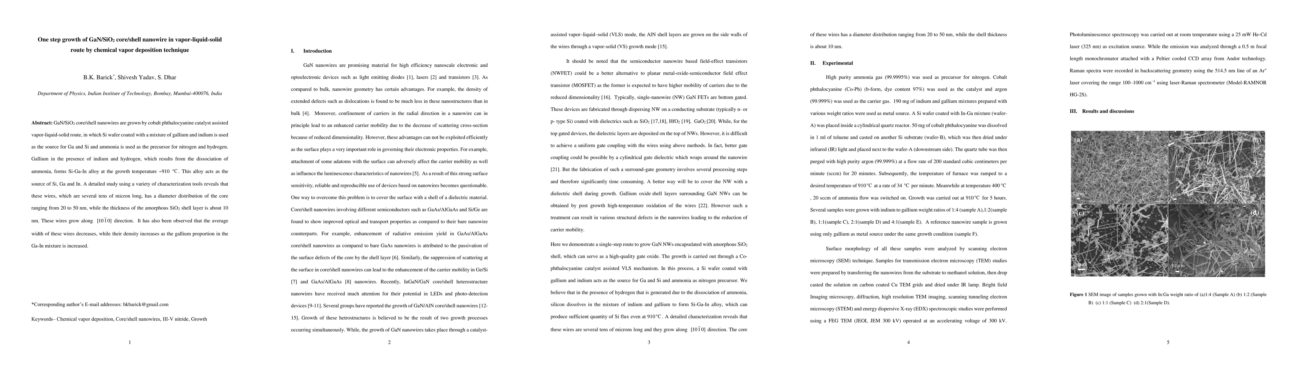
PDF Preview
Key Terms
Citation Network
Current paper (gray), citations (green), references (blue)
Display is limited for performance on very large graphs.
Similar Papers
Found 4 papers| Title | Authors | Year | Actions |
|---|
Comments (0)