Optical Band Engineering of Monolayer WSe2 in a Scanning Tunneling Microscope

Source: ArXiv

AI Quick Summary

This study employs optical-scanning tunneling microscopy (optical-STM) with near-field CW laser excitation to measure electronic changes in monolayer WSe2, showing that the tunneling gap and density of states are significantly affected by the laser intensity when resonant with the semiconductor's bandgap, indicating potential for nanoscale engineering of quantum material electronic states.

Share: Share on X LinkedIn

Summary

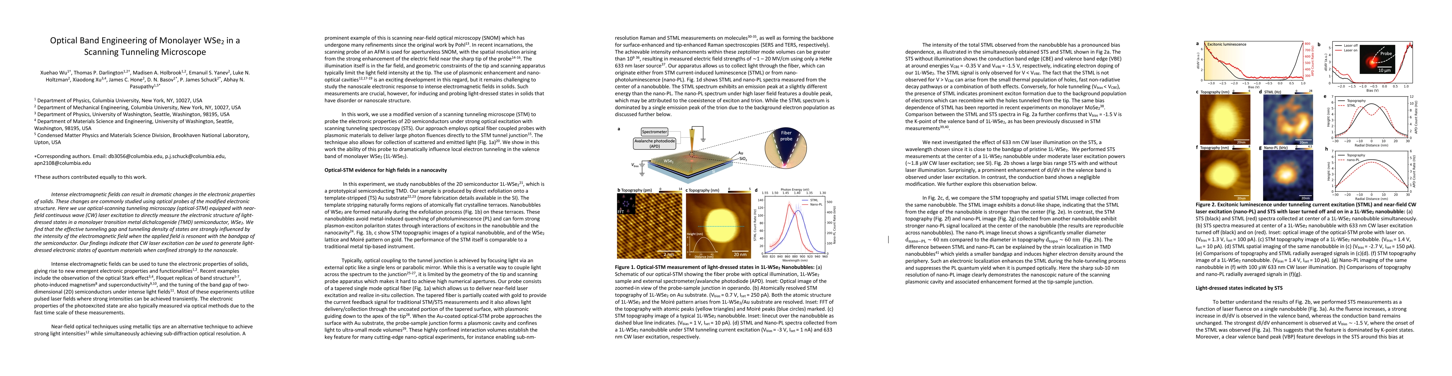
Intense electromagnetic fields can result in dramatic changes in the electronic properties of solids. These changes are commonly studied using optical probes of the modified electronic structure. Here we use optical-scanning tunneling microscopy (optical-STM) equipped with near-field continuous wave (CW) laser excitation to directly measure the electronic structure of light-dressed states in a monolayer transition metal dichalcogenide (TMD) semiconductor, WSe2. We find that the effective tunneling gap and tunneling density of states are strongly influenced by the intensity of the electromagnetic field when the applied field is resonant with the bandgap of the semiconductor. Our findings indicate that CW laser excitation can be used to generate light-dressed electronic states of quantum materials when confined strongly to the nanoscale.

AI Key Findings

Generated Sep 07, 2025

Methodology

The research utilized optical-scanning tunneling microscopy (optical-STM) equipped with near-field continuous wave (CW) laser excitation to directly measure the electronic structure of light-dressed states in a monolayer transition metal dichalcogenide (TMD) semiconductor, WSe2.

Key Results

  • The effective tunneling gap and tunneling density of states are strongly influenced by the intensity of the electromagnetic field when the applied field is resonant with the bandgap of the semiconductor.
  • CW laser excitation can be used to generate light-dressed electronic states of quantum materials when confined strongly to the nanoscale.
  • The observed enhancement of valence band dI/dV is dependent on the wavelength of light used, suggesting a resonance effect is at play.
  • Numerical simulation of STS reveals that changes in the effective mass of the valence band can effectively flatten out the top of the valence band.

Significance

The research demonstrates the electroluminescence and nano-PL nature of 1L-WSe2 nanobubbles and investigates effects of light-dressing on the 2D electronic states.

Technical Contribution

The research introduces a new method for studying light-dressed electronic states using optical-STM, providing insights into the effects of electromagnetic fields on TMD semiconductors.

Novelty

The work presents novel findings on the effects of CW laser excitation on the electronic structure of WSe2 nanobubbles, demonstrating the potential for CW optical band engineering in quantum materials.

Limitations

  • Thermal effects are not at play, as no difference in atomic scale STM topography of nanobubbles is observed at different laser fluences.
  • Photocurrent artifact cannot explain the changes to the valence band edge.

Future Work

  • Further investigation into the mechanisms behind the observed enhancement of valence band dI/dV and its dependence on wavelength.
  • Exploring the potential applications of CW optical band engineering in quantum materials.

Paper Details

PDF Preview

Download PDF

No citations found for this paper.

Comments (0)

This website uses cookies to ensure you get the best experience. Learn more