Summary
The recent discovery of sliding ferroelectricity has sparked intense interests in studying interfacial polarizations in two-dimensional (2D) van der Waals materials. However, akin to the conventional ferroelectrics, the studies have predominantly reported semiconducting and/or insulating moir\'e systems and binary compounds. Spontaneous electric polarizations in elemental metallic phases remain scarcity. Here, we report the first optical imaging of intrinsic out-of-plane electric polarizations and domain wall (DW) sliding dynamics in tetralayer graphene, a 2D conductive layer composed entirely of carbon. Using scanning near-field optical microscopy (SNOM), we directly visualize adjacent ABAC and ABCB stacking orders with intrinsic and opposite electric polarizations. Our gate-dependent SNOM measurements reveal distinct optical response that systematically changes upon carrier doping and unconventional interplay between DW sliding and electric polarizations, which are supported by density functional theory (DFT) calculations. Independent corroboration through Kelvin probe force microscopy (KPFM) and Raman spectroscopy confirms the polar nature and their polarization directions. Furthermore, reversible mechanical switching of polar states via atomic force microscopy (AFM) tip manipulation is also demonstrated. Our work establishes SNOM as a critical tool for probing sliding ferroelectricity in conductive 2D layers, opening avenues for exploring multiferroic behaviors and nonvolatile memory applications in atomically thin metals at room temperature.
AI Key Findings
Generated Jun 09, 2025
Methodology
The research utilized scanning near-field optical microscopy (SNOM), density functional theory (DFT) calculations, Kelvin probe force microscopy (KPFM), Raman spectroscopy, and atomic force microscopy (AFM) tip manipulation to directly visualize and analyze the electric polarizations and domain wall sliding dynamics in tetralayer graphene.
Key Results
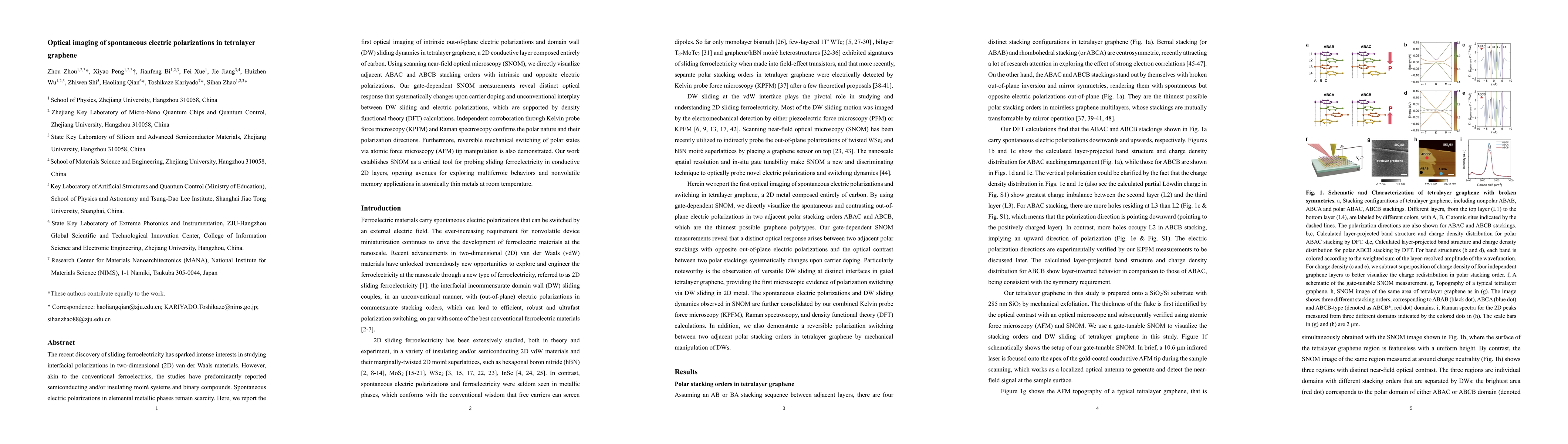
- First optical imaging of intrinsic out-of-plane electric polarizations and domain wall sliding dynamics in tetralayer graphene.
- Distinct optical response upon carrier doping, revealing unconventional interplay between domain walls and electric polarizations.
- Independent confirmation of polar nature and polarization directions through KPFM and Raman spectroscopy.
- Demonstration of reversible mechanical switching of polar states via AFM tip manipulation.
- Establishment of SNOM as a critical tool for probing sliding ferroelectricity in conductive 2D layers.
Significance
This work is significant as it reports the first optical imaging of spontaneous electric polarizations in a conductive 2D material, paving the way for exploring multiferroic behaviors and nonvolatile memory applications in atomically thin metals at room temperature.
Technical Contribution
The development and application of SNOM for direct visualization of electric polarizations and domain walls in tetralayer graphene, supported by DFT calculations and corroborated by KPFM and Raman spectroscopy.
Novelty
This research is novel due to its first-time optical imaging of intrinsic electric polarizations in a purely metallic 2D material, tetralayer graphene, and its demonstration of sliding ferroelectricity in such a system.
Limitations
- Study was limited to tetralayer graphene; further research needed to generalize findings to other 2D materials.
- Theoretical calculations relied on DFT, which may not fully capture all complexities of real materials.
Future Work
- Investigate similar phenomena in other 2D materials to establish broader applicability.
- Explore the potential for integrating these findings into practical device designs for memory and sensing applications.
Paper Details
PDF Preview
Citation Network
Current paper (gray), citations (green), references (blue)
Display is limited for performance on very large graphs.
Similar Papers
Found 4 papersInteraction-driven spontaneous broken-symmetry insulator and metals in ABCA tetralayer graphene
Kai Liu, Takashi Taniguchi, Kenji Watanabe et al.
Spontaneous spin superconductor state in ABCA-stacked tetralayer graphene
Shuai Li, Hua Jiang, Yuan-Hang Ren et al.
Spectroscopic signatures of tetralayer graphene polytypes
Zachary A. H. Goodwin, Aitor Garcia-Ruiz, Andrew McEllistrim et al.
Experimental observation of ABCB stacked tetralayer graphene
Ammon Fischer, Lennart Klebl, Dante M. Kennes et al.
No citations found for this paper.
Comments (0)