01
MethodologyHow they did it
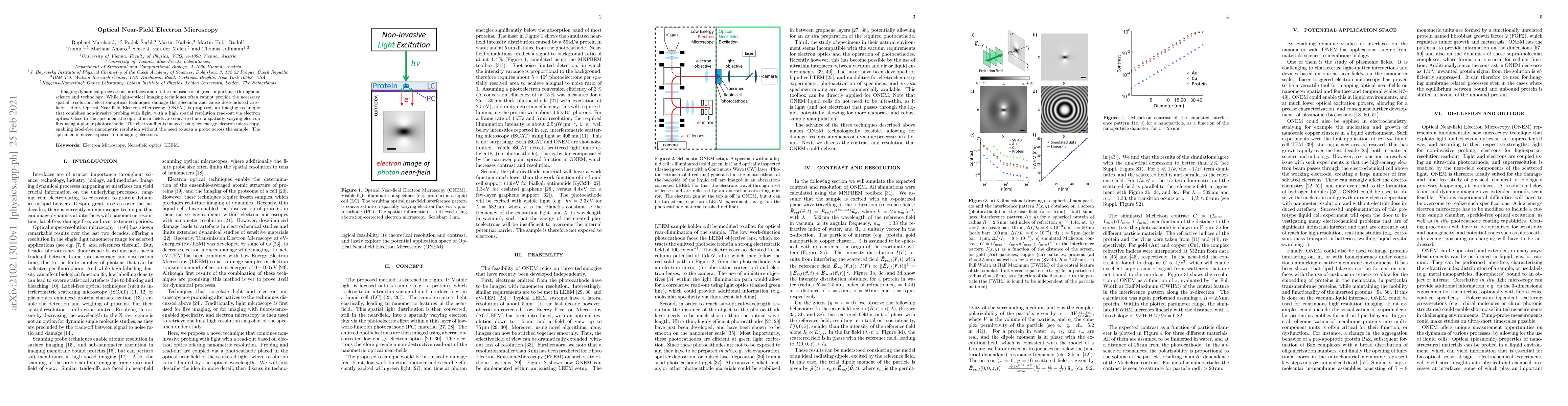
The research proposes Optical Near-Field Electron Microscopy (ONEM), a technique that combines non-invasive probing with light and high spatial resolution read-out via electron optics. It uses a planar photocathode to convert optical near-fields into a spatially varying electron flux, which is then imaged using low energy electron microscopy.
Discussion 0