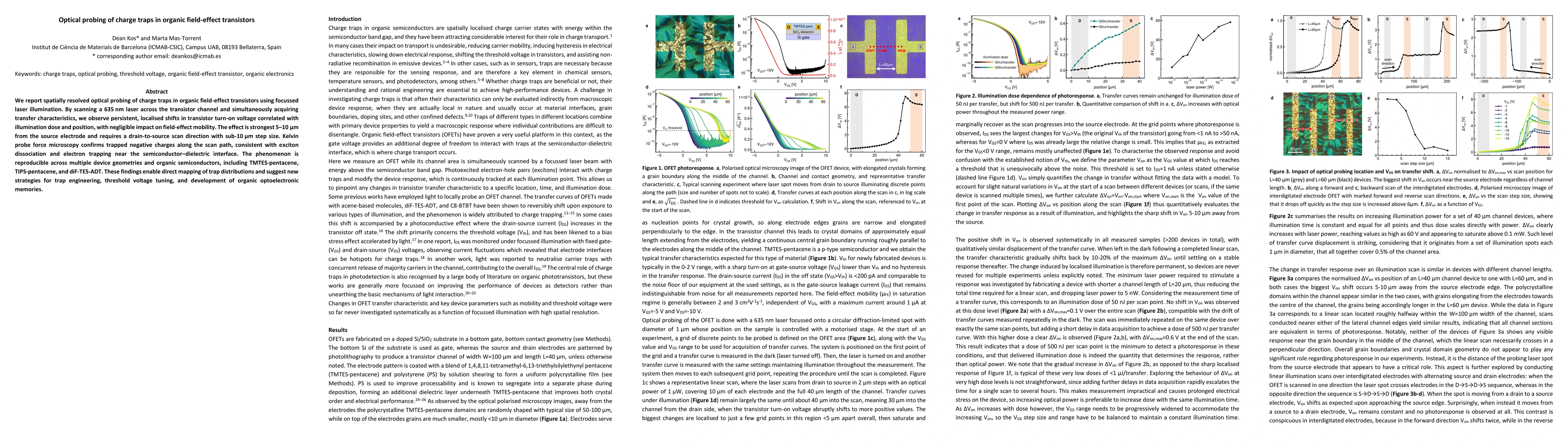
We report spatially resolved optical probing of charge traps in organic
field-effect transistors using focussed laser illumination. By scanning a 635
nm laser across the transistor channel and simultaneously acquiring transfer
characteristics, we observe persistent, localised shifts in transistor turn-on
voltage correlated with illumination dose and position, with negligible impact
on field-effect mobility. The effect is strongest 5-10 um from the source
electrode and requires a drain-to-source scan direction with sub-10 um step
size. Kelvin probe force microscopy confirms trapped negative charges along the
scan path, consistent with exciton dissociation and electron trapping near the
semiconductor-dielectric interface. The phenomenon is reproducible across
multiple device geometries and organic semiconductors, including
TMTES-pentacene, TIPS-pentacene, and diF-TES-ADT. These findings enable direct
mapping of trap distributions and suggest new strategies for trap engineering,
threshold voltage tuning, and development of organic optoelectronic memories.
Discussion 0