Orbital design of topological insulators from two-dimensional semiconductors
Publication
Metrics
Paper Preview
Abstract
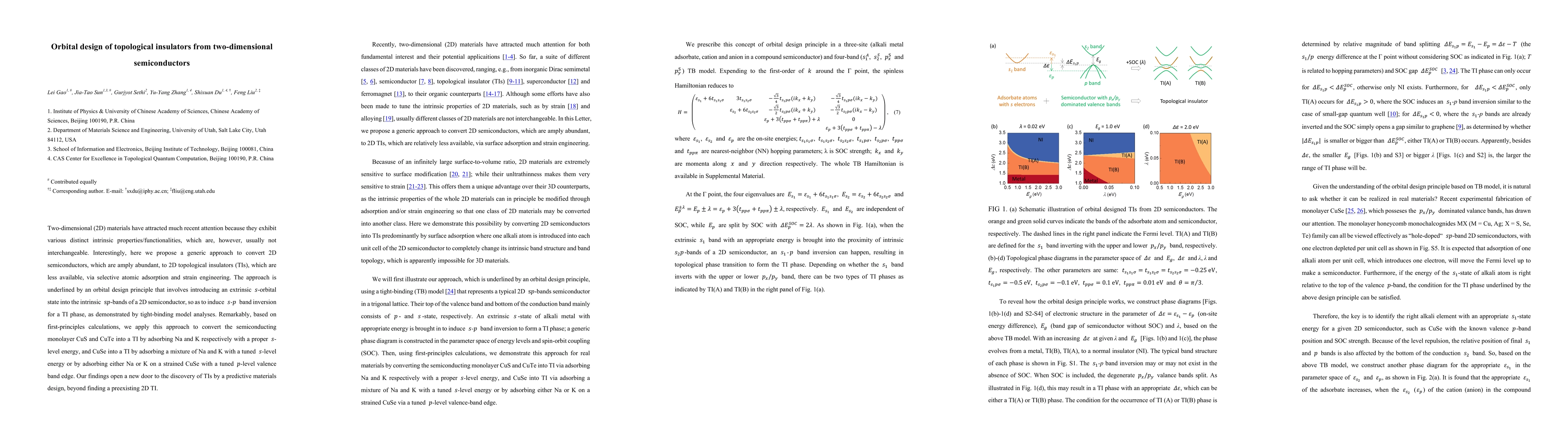
Two-dimensional (2D) materials have attracted much recent attention because they exhibit various distinct intrinsic properties/functionalities, which are, however, usually not interchangeable. Interestingly, here we propose a generic approach to convert 2D semiconductors, which are amply abundant, to 2D topological insulators (TIs), which are less available, via selective atomic adsorption and strain engineering. The approach is underlined by an orbital design principle that involves introducing an extrinsic s-orbital state into the intrinsic sp-bands of a 2D semiconductor, so as to induce s-p band inversion for a TI phase, as demonstrated by tight-binding model analyses. Remarkably, based on first-principles calculations, we apply this approach to convert the semiconducting monolayer CuS and CuTe into a TI by adsorbing Na and K respectively with a proper s-level energy, and CuSe into a TI by adsorbing a mixture of Na and K with a tuned s-level energy or by adsorbing either Na or K on a strained CuSe with a tuned p-level valence band edge. Our findings open a new door to the discovery of TIs by a predictive materials design, beyond finding a preexisting 2D TI.
AI Key Findings
Get AI-generated insights about this paper's methodology, results, significance, and more — seven facets brought into focus.
Impact
Paper Details
PDF Preview
Key Terms
Citation Network
Current paper (gray), citations (green), references (blue)
Display is limited for performance on very large graphs.
Discussion 0