Summary
2D bismuth oxyselenide (Bi2O2Se) with high electron mobility shows great potential for nanoelectronics. Although in-plane properties of Bi2O2Se have been widely studied, its out-ofplane electrical transport behavior remains elusive, despite its importance in fabricating devices with new functionality and high integration density. Here, we study the out-of-plane electrical properties of 2D Bi2O2Se at nanoscale by conductive atomic force microscope. We find that hillocks with tunable heights and sizes are formed on Bi2O2Se after applying vertical electrical field. Intriguingly, such hillocks are conductive in vertical direction, resulting in a previously unknown out-of-plane resistance switching in thick Bi2O2Se flakes while ohmic conductive characteristic in thin ones. Furthermore, we observe the transformation from bipolar to stable unipolar conduction in thick Bi2O2Se flake possessing such hillocks, suggesting its potential to function as a selector in vertical devices. Our work reveals unique out-of-plane transport behavior of 2D Bi2O2Se, providing the basis for fabricating vertical devices based on this emerging 2D material.
AI Key Findings
Get AI-generated insights about this paper's methodology, results, and significance.
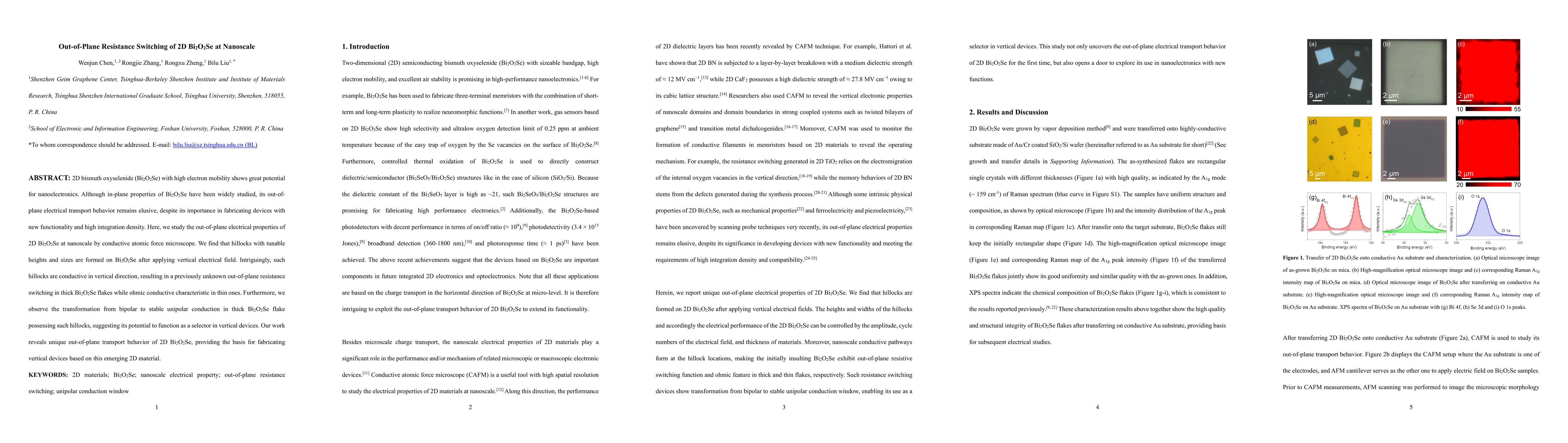
Paper Details
PDF Preview
Key Terms
Citation Network
Current paper (gray), citations (green), references (blue)
Display is limited for performance on very large graphs.
Similar Papers
Found 4 papersIn-Plane and Out-of-Plane Excitonic Coupling in 2D Molecular Crystals
Jinho Lee, Jiwon Park, Sunmin Ryu et al.
Switching of magnetic domains in a noncollinear antiferromagnet at the nanoscale
Wolfgang Hoppe, Georg Woltersdorf, Stuart S. P. Parkin et al.
| Title | Authors | Year | Actions |
|---|
Comments (0)