This study investigates O2-plasma-based digital etching of Al0.25Ga0.75N with an AlN etch-stop layer, achieving precise control over etch depth and improved surface roughness, demonstrating reduced damage compared to dry etching alone.
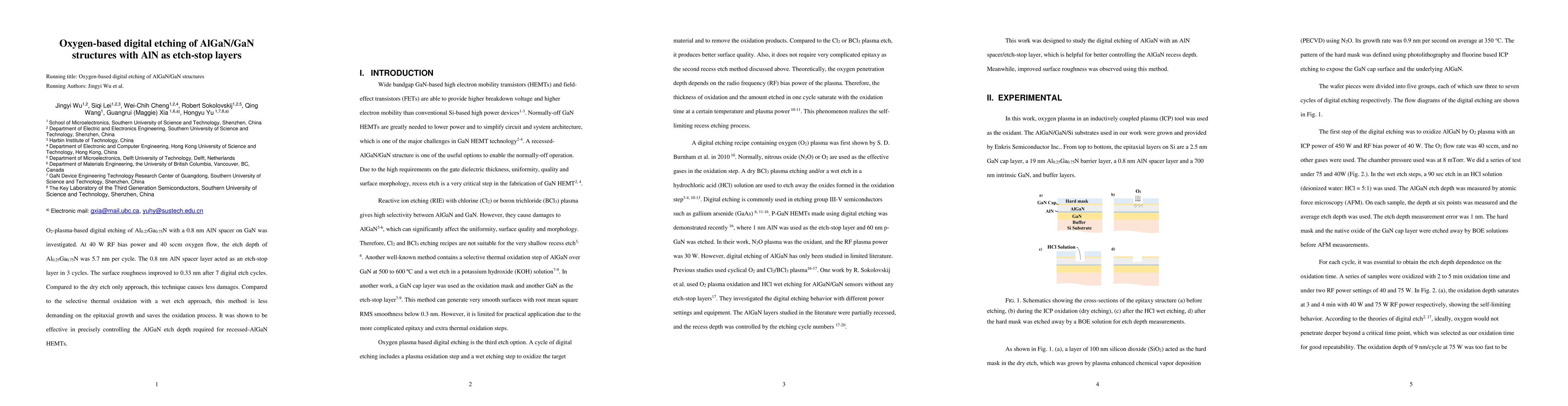
O2-plamsa-based digital etching of Al0.25Ga0.75N with a 0.8 nm AlN spacer on GaN was investigated. At 40 W RF bias power and 40 sccm oxygen flow, the etch depth of Al0.25Ga0.75N was 5.7 nm per cycle. The 0.8 nm AlN spacer layer acted as an etch-stop layer in 3 cycles. The surface roughness improved to 0.33 nm after 7 digital etch cycles. Compared to the dry etch only approach, this technique causes less damages. It was shown to be effective in precisely controlling the AlGaN etch depth required for recessed-AlGaN HEMTs.
This graph shows how this paper is connected to other research. The current paper is shown in dark gray, papers that cite it are in green, and papers it references are in blue. You can:
• Hover over any node to see the paper title
• Click a node to view that paper's details
• Drag nodes to rearrange the graph
• Use the zoom controls (bottom right) to zoom in/out
Title | Authors | Year | Actions |
---|---|---|---|
Study on a p-GaN HEMT with composite passivation and composite barrier layers
|
Junji Cheng, Queyang Wang, Yikai Liu, Guo Ding, Minming Zhang, Bo Yi, Haimeng Huang, Hongqiang Yang
|
2024
|
View Paper |
Recent Developments and Prospects of Fully Recessed MIS Gate Structures for GaN on Si Power Transistors
|
P. Fernandes Paes Pinto Rocha, L. Vauche, P. Pimenta-Barros, S. Ruel, R. Escoffier, J. Buckley
|
2023
|
View Paper |
Plasma atomic layer etching of GaN/AlGaN materials and application: An overview
|
Lulu Guan, Xingyu Li, Dongchen Che, Kaidong Xu, Shiwei Zhuang
|
2022
|
View Paper |
Enhancement-Mode Multi-Channel AlGaN/GaN Transistors With LiNiO Junction Tri-Gate
|
Taifang Wang, Yuan Zong, L. Nela, E. Matioli
|
2022
|
View Paper |
Enhancement-Mode High-Frequency InAlGaN/GaN MIS-HEMT Fabricated by Implementing Oxygen-Based Digital Etching on the Quaternary Layer
|
P. Tsai, Hoang-Tan-Ngoc Nguyen, V. Nagarajan, Chun-Hsiung Lin, C. Dee, Shih-Chen Chen, H. Kuo, C. Lee, E. Chang
|
2022
|
View Paper |
The Atomic Layer Etching Technique with Surface Treatment Function for InAlN/GaN Heterostructure
|
Fangzhou Du, Yang Jiang, Zhanxia Wu, Honghao Lu, Jiaqi He, Chuying Tang, Qiaoyu Hu, Kangyao Wen, Xinyi Tang, Haimin Hong, Hongyu Yu, Qing Wang
|
2022
|
View Paper |
Control of V th of the enhancement high-frequency AlGaN/GaN HEMT fabricated by oxygen-based digital etching
|
P. Tsai, Yu Chen, Chun-Hsiung Lin, E. Chang
|
2021
|
View Paper |
Self-Align-Gated GaN Field Emitter Arrays Sharpened by a Digital Etching Process
|
Pao-Chuan Shih, G. Rughoobur, K. Cheng, A. Akinwande, T. Palacios
|
2021
|
View Paper |
Recent Advances in GaN‐Based Power HEMT Devices
|
Jiaqi He, W. Cheng, Qing Wang, K. Cheng, Hongyu Yu, Y. Chai
|
2021
|
View Paper |
Etch-stop process for precisely controlling the vertical cavity length of GaN-based devices
|
Yen-Yu Liu, Tsung-Che Wu, P. Yeh
|
2020
|
View Paper |
Digital etching of AlGaN/GaN heterostructures with GaN cap using inductively coupled oxygen plasma process combined with wet chemical treatment
|
Jong-Hee Kim, Hyeon-Cheol Kim, Hyeon-Yeong Jeong, V. Janardhanam, A. A. Kumar, V. Rajagopal Reddy, Chel-Jong Choi
|
2024
|
View Paper |
Investigation of AlGaN/GaN Schottky Barrier Diodes on Free-Standing GaN Substrate with low leakage current
|
Wu Peng Zhang Tao, Zhang Jincheng, Hao Yue
|
2022
|
View Paper |
Development of a Monolithically Integrated GaN Nanowire Memory Device
|
Vijay Gopal, T. Vangipuram, Jing Zhang, Bryan Melanson
|
2021
|
View Paper |
Nick Pant, Emmanouil Kioupakis, Woncheol Lee, Nocona Sanders
Published: 2022-08-10
Daosheng Tang, Limin Zhang
Published: 2023-07-21
Published: 2021-07-28
E. Monroy, E. Akar, I. Dimkou, A. Ajay, Martien I. den Hertog
Published: 2023-07-17
Comments (0)